


PXA250 and PXA210 Applications Processors Design Guide 9-1
JTAG/Debug Port 9
9.1 Description
The JTAG/Debug port is essentially several shift registers, with the destination controlled by the
TMS pin and data I/O with TDI/TDO. nTRST provides initialization of the test logic. JTAG is
testable via the IEEE 1149.1. Many use JTAG to control the address/data bus for Flash
programming. JTAG is also a hardware debug port.
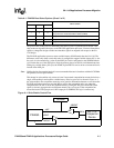
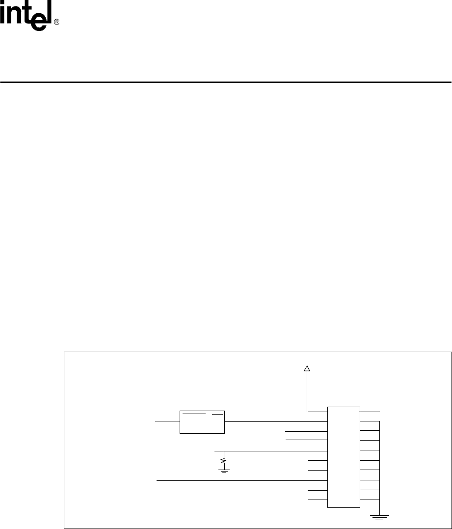
9.2 Schematics
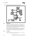
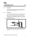
All JTAG pins, except for nTRST and TCK, are directly connected. TCK is not driven internally
and so you must add an external pull-up or pull-down resistor. Intel recommends adding a 1.5 k
pull-down resistor to TCK. nTRST must be asserted during power-on. Asserting nRESET or
nTRST must not cause the other reset signal to assert. Also, use an external pull-up resistor on
nTRST to prevent spurious resets of the JTAG port when disconnected. The circuit in Figure 9-1
drives nTRST. It uses a reset IC on nTRST to ensure that nTRST is reset at power-on. nRESET
must be directly connected to the CPU nRESET. Do not connect pins 17 and 19 – they are special
purpose functions and not used.
If you are not utilizing either JTAG or the hardware debug functions, it is highly recommended that
you design in a JTAG/debug port on your system anyway. This greatly facilitates board debug,
startup, and software development. During final production you would not have to populate the
JTAG connector.
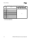
Figure 9-1. JTAG/Debug Port Wiring Diagram
MAX823
RESET
MR
1
3
5
7
9
11
13
15
17
19
2
4
6
8
10
12
14
16
18
20
3.3 V
1.5K
TDO
TCK
TDI
TMS
nTRST
nRESET
GND