


PXA250 and PXA210 Applications Processors Design Guide 2-17
System Memory Interface
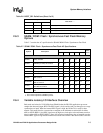
2.7 System Memory Layout Guidelines
2.7.1 System Memory Topologies (Min and Max Simulated
Loading)
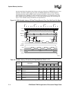
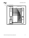
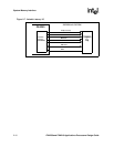
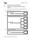
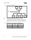
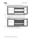
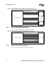
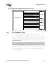
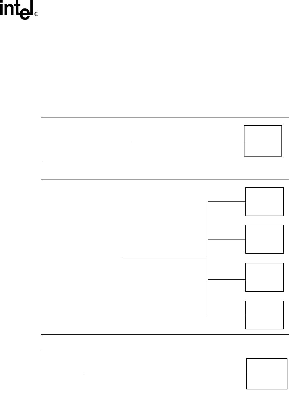
Figure 2-8, Figure 2-9, Figure 2-10, and Figure 2-11 are the topologies that where simulated to
develop the trace length recommendations in Section 2.7.2. These topologies are for reference
only.
Figure 2-8. CS, CKE, DQM, CLK, MA minimum loading topology
Figure 2-9. CS, CKE, DQM, CLK, MA Maximum Loading Topology
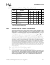
Figure 2-10. MD Minimum Loading Topology
CS, CKE, DQM,
CLK, MA
SDRAM
SDRAM
SDRAM
SDRAM
SDRAM
CS, CKE, DQM,
CLK, MA
MD
SDRAM