


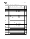
PXA250 and PXA210 Applications Processors Design Guide 8-13
Power and Clocking
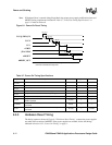
8.5.4 Watchdog Reset Timing
Watchdog Reset is an internally generated reset and therefore has no external pin dependencies.
The nRESET_OUT pin is the only indicator of Watchdog Reset, and it stays asserted for
t
DHW_OUT
. Refer to Figure 8-2, “Hardware Reset Timing” on page 8-13 for more information.
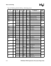
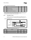
8.5.5 GPIO Reset Timing
GPIO Reset is generated externally. The pin used as the GPIO Reset is reconfigured as a standard
GPIO after the reset propagates internally. Because the clock module is not reset by GPIO Reset,
timing varies based on the frequency of the selected clock. Timing also varies in the Frequency
Change Sequence (see Section 8.4.1, “32.768 kHz Oscillator Specifications” on page 4). Figure
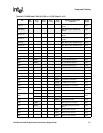
8-3 “GPIO Reset Timing” shows the possible GPIO Reset timing.
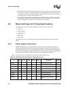
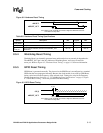
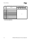
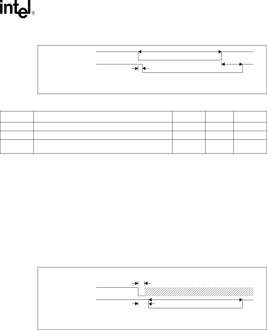
Figure 8-2. Hardware Reset Timing
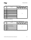
Table 8-8. Hardware Reset Timing Specifications
Symbol Description Min Typical Max
t
DHW_NRESET
Minimum assertion time of nRESET 0.001 ms — —
t
DHW_OUT_A
Delay between nRESET Asserted and nRESET_OUT Asserted 0ms — 0.001 ms
t
DHW_OUT
Delay between nRESET deasserted and nRESET_OUT
deasserted
18.1 ms — 18.2 ms
nRESET
nRESET_OUT
t
DHW_NRESET
t
DHW_OUT
Note: nBATT_FAULT and nVDD_FAULT must be high before nRESET is deasserted
or PXA250 enters Sleep Mode
t
DHW_OUT_A
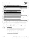
Figure 8-3. GPIO Reset Timing
GP[1]
nRESET_OUT
t
A_GP[1]
t
DGP_OUT
Note: nBATT_FAULT and nVDD_FAULT must be high before nRESET is deasserted
or PXA250 enters Sleep Mode
t
DGP_OUT_A