


8-12 PXA250 and PXA210 Applications Processors Design Guide
Power and Clocking
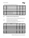
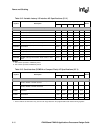
Note: If Hardware Reset is entered during Sleep Mode, the proper power-supply stabilization times and
nRESET timing requirements indicated in Table 8-7, “Power-On Timing Specifications” on
page 8-12 must be observed.
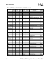
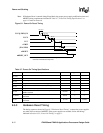
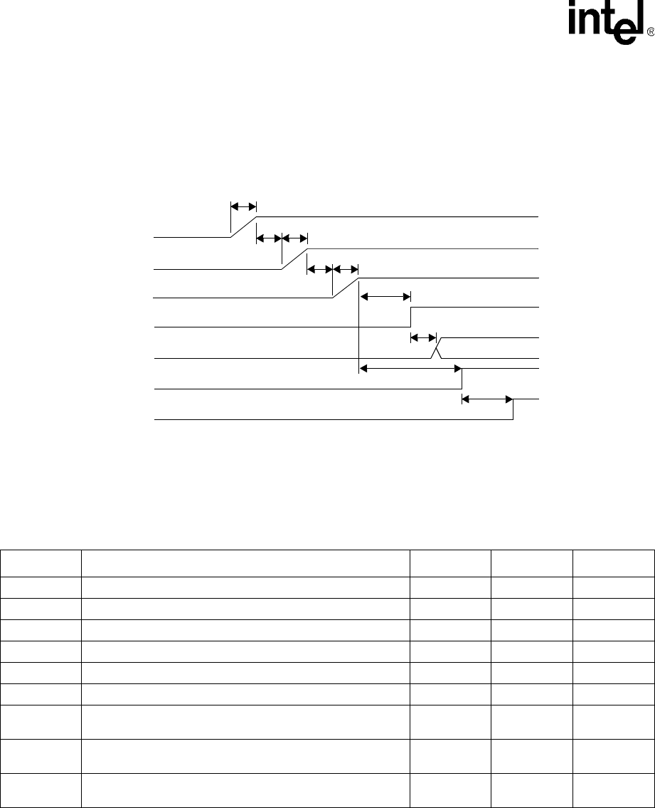
Figure 8-1. Power-On Reset Timing
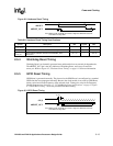
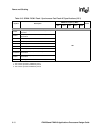
8.5.3 Hardware Reset Timing
The timing sequences shown in Figure 8-2 “Hardware Reset Timing” assumes the power supplies
are stable at the assertion of nRESET. If the power supplies are unstable, follow the timings
indicated in Section 8.5.2, “Power On Timing” on page 11.
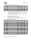
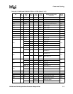
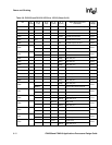
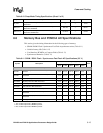
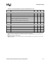
Table 8-7. Power-On Timing Specifications
Symbol Description Min Typical Max
t
R_VCCQ
VCCQ Rise / Stabilization time 0.01 ms — 100 ms
t
R_VCCN
VCCN Rise / Stabilization time 0.01 ms — 100 ms
t
R_VCC
VCC, PLL_VCC Rise / Stabilization time 0.01 ms — 10 ms
t
D_VCCN
Delay between VCCQ stable and VCCN applied 0ms — —
t
D_VCC
Delay from VCCN stable and VCC, PLL_VCC applied 0ms — —
t
D_NTRST
Delay between VCC, PLL_VCC stable and nTRST deasserted 50 ms — —
t
D_JTAG
Delay between nTRST deasserted and JTAG pins active, with
nRESET asserted
0.03 ms — —
t
D_NRESET
Delay between VCC, PLL_VCC stable and nRESET
deasserted
50 ms — —
t
D_OUT
Delay between nRESET deasserted and nRESET_OUT
deasserted
18.1 ms — 18.2 ms
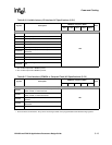
VCCQ, PWR_EN
VCC
nTRST
JTAG PINS
nRESET
nRESET_OUT
t
R_VCCQ
t
R_VCC
t
D_VCC
t
D_NTRST
t
D_JTAG
t
D_NRESET
t
D_OUT
Note: nBATT_FAULT and nVDD_FAULT must be high before nRESET_OUT is
deasserted or PXA250 enters Sleep Mode
VCCN
t
R_VCCN
t
D_VCCN