


PXA250 and PXA210 Applications Processors Design Guide 2-11
System Memory Interface
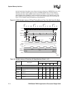
2.6.5 External Logic for PCMCIA Implementation
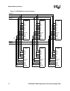
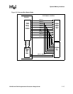
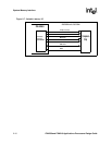
The PXA250 applications processor requires external glue logic to complete the PCMCIA socket
interface. Figure 2-4, “Expansion Card External Logic for a Two-Socket Configuration” on page 2-
12 and Figure 2-5, “Expansion Card External Logic for a One-Socket Configuration” on page 2-13
show general solutions for one and two socket configurations. Use GPIO or memory-mapped
external registers to control the PCMCIA interface’s reset, power selection (V
CC
and V
PP
), and
drive enables. These diagrams show the logical connections necessary to support hot insertion
capability. For dual-voltage support, level shifting buffers are required for all the applications
processor input signals. Hot insertion capability requires each socket be electrically isolated from
the other and from the remainder of the memory system. If one or both of these features are not
required, you may eliminate some of the logic shown in these diagrams. The applications processor
allows either 1-socket or 2-socket solutions. In the 1-socket solution, only minimal glue logic is
required (typically for the data transceivers, address buffers, and level shifting buffers.) To achieve
this some of the signals are routed through dual-duty GPIO pins. The nOE of the transceivers is
driven through the PSKTSEL pin, which is not needed in the one-socket solution. The DIR pin of
the transceiver is driven through the RDnWR pin. A GPIO is used for the three-state signal of the
address and nPWE lines. These signals are used for memories other than the card interface and
must be three-stated.
Note: For 2.5 V VCCN, 5 V to 2.5 V level shifters are required.
Note: PCMCIA is only implemented on the PXA250 applications processor.
In the 2-socket solution, all pins assume their normal duties and glue logic is necessary for proper
operation of the system. The pull-ups shown are included for compliance with PC Card Standard -
Volume 2 - Electrical Specification. Remove power from these pull-ups during sleep to avoid
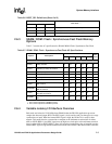
unnecessary power consumption. Refer to Table 2-9 for the PCMCIA or compact Flash card
interface AC specifications.
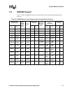
tvlioDSW
MD(31:0), DQM(3:0) write data setup to
nPWE asserted
10 8.5 7.5 6.8 6 ns, 1
tvlioDSWH
MD(31:0), DQM(3:0) write data setup to
nPWE de-asserted
20 17 15 13.6 12 ns, 2
tvlioDHW
MD(31:0), DQM(3:0) hold after nPWE
de-asserted
10 8.5 7.5 6.8 6 ns, 1
tvlioDHR
MD(31:0) read data hold after nOE de-
asserted
00000ns
tvlioRDYH
RDY hold after nOE, nPWE de-
asserted
00000ns
tvlioNPWE
nPWE, nOE high time between beats of
write or read data
20 17 15 13.6 12 ns, 2
NOTES:
1. This number represents 1 MEMCLK period
2. This number represents 2 MEMCLK periods
Table 2-8. Variable Latency I/O Interface AC Specifications (Sheet 2 of 2)
Symbol Description
MEMCKLK
Units
Notes
99.5 118.0 132.7 147.5 165.9