


A-2 PXA250 and PXA210 Applications Processors Design Guide
SA-1110/Applications Processor Migration
— Intel® XScale™ microarchitecture
—Debugging
- Cache attributes
- Other Features
- Conclusion
A.1 SA-1110 Hardware Migration Issues
A.1.1 Hardware Compatibility
The majority of the features provided in the SA-1110 are also provided in the PXA250 applications
processor. However, with the additional functionality of the PXA250 applications processor, the
two devices are not pin compatible and cannot occupy the same socket.
There has been an effort to ensure Companion Devices that take advantage of SA-1110 memory
interface access works with the PXA250 applications processor. The memory controls for taking
over the memory bus such as those exercised by the SA-1111, are included in the PXA250
applications processor memory bus interface however, there are some issues.
One difference in particular is the way PXA250 applications processor toggles the A1 and A0
address lines. The SA-1110 toggled A1 and A0 regardless of the size of the data bus. With
PXA250, if the data bus is set to 16-bit, then A0 does not toggle and if the data bus is set to 32-bit,
then neither A1 nor A0 toggles.
There is a big difference in manufacturing technology between the SA-1110 and the PXA250
applications processors. The most significant change being from a 0.35 micron CMOS technology
to a finer lithography of 0.18 microns. Aside from a potential impact to signal edge rates this
allows for lower applications processor voltage operation.
A.1.2 Signal Changes
There are two pins that control SA-1110 boot-up:
• ROM select pin that selects a 16 or 32-bit interface
• Synchronous Mask ROM enable pin that selects a synchronous or asynchronous ROM access
The PXA250 applications processor has three pins that select eight different boot select options
(see Table A-1. The subset of these options that are SA-1110 equivalent are not compatible with the
PXA250 applications processor pin polarities, so these pins must be selected afresh when
designing with the PXA250 applications processor.
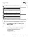
Table A-1. PXA250 Boot Select Options (Sheet 1 of 2)
Boot Select Pins
Boot Location
210
0 0 0 Asynchronous 32-bit ROM
0 0 1 Asynchronous 16-bit ROM
0 1 0 Synchronous 32-bit Flash