


PXA250 and PXA210 Applications Processors Design Guide iii
Contents
Contents
1 Introduction.................................................................................................................................1-1
1.1 Functional Overview ..........................................................................................................1-1
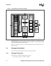
1.2 Package Information..........................................................................................................1-2
1.2.1 Package Introduction ............................................................................................1-2
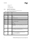
1.2.2 Signal Pin Descriptions.........................................................................................1-4
2 System Memory Interface ..........................................................................................................2-1
2.1 Overview............................................................................................................................2-1
2.2 SDRAM Interface...............................................................................................................2-3
2.3 SDRAM memory wiring diagram .......................................................................................2-3
2.4 SDRAM Support ................................................................................................................2-5
2.5 SDRAM Address Mapping.................................................................................................2-6
2.6 Static Memory....................................................................................................................2-7
2.6.1 Overview...............................................................................................................2-7
2.6.2 Boot Time Defaults ...............................................................................................2-8
2.6.3 SRAM / ROM / Flash / Synchronous Fast Flash Memory Options .......................2-9
2.6.4 Variable Latency I/O Interface Overview ..............................................................2-9
2.6.5 External Logic for PCMCIA Implementation .......................................................2-11
2.6.6 DMA / Companion Chip Interface .......................................................................2-14
2.7 System Memory Layout Guidelines .................................................................................2-17
2.7.1 System Memory Topologies (Min and Max Simulated Loading).........................2-17
2.7.2 System Memory Recommended Trace Lengths.................................................2-18
3 LCD Display Controller ..............................................................................................................3-1
3.1 LCD Display Overview.......................................................................................................3-1
3.2 Passive (DSTN) Displays ..................................................................................................3-1
3.2.1 Typical Connections for Passive Panel Displays..................................................3-2
3.2.1.1 Passive Monochrome Single Panel Displays........................................3-2
3.2.1.2 Passive Monochrome Single Panel Displays, Double-Pixel Data.........3-3
3.2.1.3 Passive Monochrome Dual Panel Displays ..........................................3-3
3.2.1.4 Passive Color Single Panel Displays ....................................................3-4
3.2.1.5 Passive Color Dual Panel Displays.......................................................3-4
3.3 Active (TFT) Displays ........................................................................................................3-5
3.3.1 Typical connections for Active Panel Displays......................................................3-6
3.4 PXA250 Pinout ..................................................................................................................3-7
3.5 Additional Design Considerations......................................................................................3-8
3.5.1 Contrast Voltage ...................................................................................................3-8
3.5.2 Backlight Inverter ..................................................................................................3-8
3.5.3 Signal Routing and Buffering ................................................................................3-8
3.5.4 Panel Connector ...................................................................................................3-9
4 USB Interface ..............................................................................................................................4-1
4.1 Self Powered Device .........................................................................................................4-1
4.1.1 Operation if GPIOn and GPIOx are Different Pins................................................4-1
4.1.2 Operation if GPIOn and GPIOx are the Same Pin................................................4-2
4.2 Bus Powered Device .........................................................................................................4-2