


1-2 PXA250 and PXA210 Applications Processors Design Guide
Introduction
s
The PXA250 applications processor package is: 256 pin, 17x17 mBGA – 32-bit functionality. The
PXA210 applications processor package is: 225 pin, 13x13 MMAP – 16-bit functionality, a subset
of the PXA250 applications processor feature set.
Section 1.2.1, “Package Introduction” contains a breakdown of the features supported by the two
different packages.
1.2 Package Information
This section describes the package types, pinouts, and signal descriptions.
1.2.1 Package Introduction
Package features of the PXA250 applications processor are:
• Core frequencies supported - 100 MHz - 400 MHz
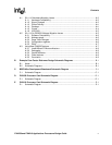
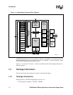
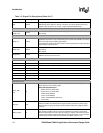
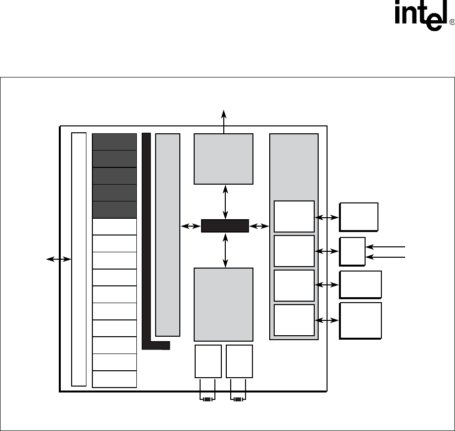
Figure 1-1. Applications Processor Block Diagram
A8651-01
Megacell
Core
Color or
Grayscale
LCD
Controller
RTC
OS Timer
PWM(2)
Int.
Controller
Clocks &
Power Man.
I
2
S
AC97
UART1
UART2
Slow IrDA
SSP
USB
Client
General Purpose I/O
ASIC
Socket 0
Socket 1
3.6864
MHz
Osc
32.768
KHz
Osc
DMA Controller
and Bridge
XCVR
SDRAM/
SMROM
4 banks
ROM/
Flash/
SRAM
4 banks
I
2
C
Fast IrDA
MMC
Peripheral Bus
System Bus
Memory
Controller
Variable
Latency I/O
Control
PCMCIA
& CF
Control
Dynamic
Memory
Control
Static
Memory
Control