


PXA250 and PXA210 Applications Processor Design Guide 3-7
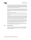
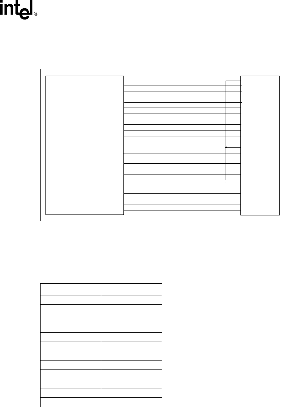
LCD Display Controller
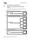
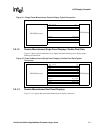
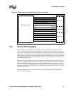
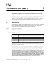
Note: This example shows 6 red, 6 green and 6 blue bits on the LCD panel. However, different active
display panels might have more or different data lines. Consult the LCD panel manufacturer’s
datasheet for the actual data lines.
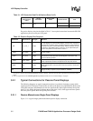
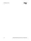
3.4 PXA250 Pinout
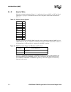
Table 3-4 describes the ball positions for the LCD controller on the PXA250 applications
processor.
Figure 3-6. Active Color Display Typical Connection
PXA250 Processor
LCD Panel
L_DD0
L_DD1
L_DD2
L_DD3
L_DD4 - MSB of Blue
L_DD5
L_DD6
L_DD7
L_PCLK
L_LCLK
L_FCLK
L_BIAS
L_DD8
L_DD9
L_DD10 - MSB of Green
L_DD11
L_DD12
L_DD13
L_DD14
L_DD15 - MSB of Red
B1
B2
B3
B4
B5
G0
G1
G2
G3
G4
G5
R0
R1
R2
R3
R4
Clock
Horizontal Sync
Vertical Sync
Data Enable
R5
B0
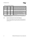
Table 3-4. PXA250 LCD Controller Ball Positions (Sheet 1 of 2)
Pin Name Ball Position
L_DD0 E7
L_DD1 D7
L_DD2 C7
L_DD3 B7
L_DD4 E6
L_DD5 D6
L_DD6 E5
L_DD7 A6
L_DD8 C5
L_DD9 A5
L_DD10 D5
L_DD11 A4