


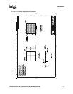
PXA250 and PXA210 Applications Processors Design Guide 1-9
Introduction
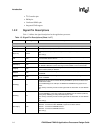
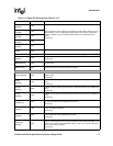
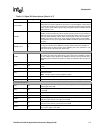
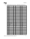
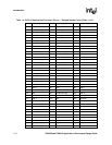
nVDD_FAULT IC
VDD Fault. Active low input.
nVDD_FAULT causes the applications processor
to enter Sleep Mode. nVDD_FAULT
is ignored after a wakeup event until the power supply timer completes (approximately
10 ms). use the nVDD_FAULT signal to flag a low battery. Minimum assertion time for
nVDD_FAULT is 1 ms.
nRESET IC
Hard reset. Active low input.
nRESET is a level sensitive input which starts the processor from a known address. A
LOW level causes the current instruction to terminate abnormally, and all on-chip state
to be reset. When nRESET is driven HIGH, the processor re-starts from address 0.
nRESET must remain LOW until the power supply is stable and the internal 3.6864
MHz oscillator has come up to speed. While nRESET is LOW the processor performs
idle cycles.
nRESET_OUT OC
Reset Out. Active low output.
This signal is asserted when nRESET is asserted and de-asserts after nRESET is
negated but before the first instruction fetch. nRESET_OUT is also asserted for “soft”
reset events (sleep, watchdog reset, GPIO reset)
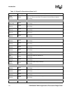
JTAG Pins
nTRST IC
JTAG Test Interface Reset. Resets the JTAG/Debug port. If JTAG/Debug is used,
drive nTRST from low to high either before or at the same time as nRESET. If JTAG is
not used, nTRST must be either tied to nRESET or tied low. Intel recommends that a
JTAG/Debug port be added to all systems for debug and download. See Chapter 9 for
details.
TDI IC JTAG test interface data input. Note this pin has an internal pullup resistor.
TDO OCZ
JTAG test interface data output. Note this pin does NOT have an internal pullup
resistor.
TMS IC JTAG test interface mode select. Note this pin has an internal pullup resistor.
TCK IC
JTAG test interface reference Clock. TCK is the reference clock for all transfers on the
JTAG test interface.
NOTE: This pin needs an external pulldown resistor.
TEST IC Test Mode. You should ground this pin. This pin is for manufacturing purposes only.
TESTCLK IC Test Clock. Use this pin for test purposes only. An end user should ground this pin.
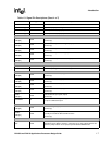
Power and Ground Pins
VCC SUP
Positive supply for the internal logic. Connect this supply to the low voltage (.85 -
1.65v) supply on the PCB.
VSS SUP
Ground supply for the internal logic. Connect these pins to the common ground plane
on the PCB.
PLL_VCC SUP Positive supply for PLLs and oscillators must be shorted to VCC.
PLL_VSS SUP Ground supply for the PLL. Must be connected to common ground plane on the PCB.
VCCQ SUP
Positive supply for all CMOS I/O except memory bus and PCMCIA pins. Connect
these pins to the common 3.3v supply on the PCB.
VSSQ SUP
Ground supply for all CMOS I/O except memory bus and PCMCIA pins. Connect
these pins to the common ground plane on the PCB.
VCCN SUP
Positive supply for memory bus and PCMCIA pins. Connect these pins to the common
3.3 V or 2.5 V supply on the PCB.
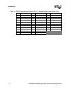
Table 1-3. Signal Pin Descriptions (Sheet 6 of 7)
Name Type Description