


PXA250 and PXA210 Applications Processors Design Guide B-1
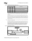
Example Form Factor Reference Design
Schematic Diagrams B
B.1 Notes
The example form factor reference design schematics in this appendix have known issues and
assumptions that need to be assessed for each board design. This appendix documents the issues
that have been discovered and provides revision data for the schematics. This appendix also points
out some of the design specific assumptions that were made in designing this board.
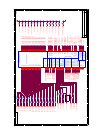
Page 4: The schematic supports the SA1110 legacy mode for addressing the SDRAM. See
SDRAM section of the design guidelines to explain normal vs. legacy addressing modes.
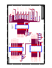
Page 10: U26 allows the CF card to access the I
2
C interface.
Page 11: The MMC slot has resistor jumpers to select SDCARD and/or MMC card support. If the
users wants to support both SCARD and MMC, populate the resistor values in the SD column of
the CARD selection table. If MMC card support only populate the resistors under the MMC
column in the table.
Page 11: The JTAG port on this board assumes that it is connected to a specific JTAG bridge board.
If you follow this design guide, you should not need the bridge board. See the JTAG section of this
document for more details on this bridge board implementation.
Page 11: J19 pin 9 requires a 1.5 k pull down.
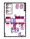
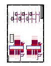
Page 13: U33, U34, U35, U40, and surrounding circuits are to support a legacy sharp LCD. Refer
to that vendor’s design guidelines if you are integrating a different LCD display.
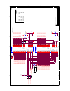
Page 14: U36, U37, U39, J13, and surrounding circuits including the resistor divider network in the
upper left hand corner support a legacy Sharp LCD. Refer to that vendor’s design guidelines if you
are integrating a different LCD display.
Page 14: J14 is the Toshiba LCD connector. Confirm the pinout before layout.
B.2 Schematic Diagrams
The example form factor reference design schematics are on the following pages.