


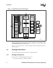

1-6 PXA250 and PXA210 Applications Processors Design Guide
Introduction
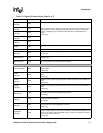
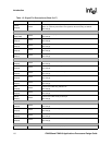
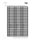
nPREG/
GPIO[55]
ICOCZ
PCMCIA register select. Output signal that indicates the target address is attribute
space, on a memory transaction. This signal has the same timing as address.
See Note [2]
LCD Controller Pins
L_DD(15:0)/
GPIO[73:58]
ICOCZ
LCD Controller display data
See Note [2]
L_FCLK/
GPIO[74]
ICOCZ
LCD Frame clock
See Note [2]
L_LCLK/
GPIO[75]
ICOCZ
LCD Line clock
See Note [2]
L_PCLK/
GPIO[76]
ICOCZ
LCD pixel clock
See Note [2]
L_BIAS/
GPIO[77]
ICOCZ
AC Bias Drive
See Note [2]
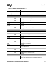
Full Function UART Pins
FFRXD/
GPIO[34]
ICOCZ
Full Function UART Receive pin
See Note [2]
FFTXD/
GPIO[39]
ICOCZ
Full Function UART Transmit pin
See Note [2]
FFCTS/
GPIO[35]
ICOCZ
Full Function UART Clear-to-Send pin
See Note [2]
FFDCD/
GPIO[36]
ICOCZ
Full Function UART Data-Carrier-Detect Pin
See Note [2]
FFDSR/
GPIO[37]
ICOCZ
Full Function UART Data-Set-Ready Pin:
See Note [2]
FFRI/
GPIO[38]
ICOCZ
Full Function UART Ring Indicator Pin
See Note [2]
FFDTR/
GPIO[40]
ICOCZ
Full Function UART Data-Terminal-Ready pin
See Note [2]
FFRTS/
GPIO[41]
ICOCZ
Full Function UART Ready-to-Send pin
See Note [2]
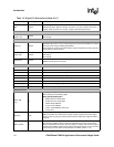
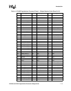
Bluetooth UART Pins
BTRXD/
GPIO[42]
ICOCZ
Bluetooth UART Receive pin
See Note [2]
BTTXD/
GPIO[43]
ICOCZ
Bluetooth UART Transmit pin
See Note [2]
BTCTS/
GPIO[44]
ICOCZ
Bluetooth UART Clear-to-Send pin
See Note [2]
BTRTS/
GPIO[45]
ICOCZ
Bluetooth UART Data-Terminal-Ready pin
See Note [2]
MMC Controller Pins
MMCMD ICOCZ Multimedia Card Command pin (I/O)
Table 1-3. Signal Pin Descriptions (Sheet 3 of 7)
Name Type Description