


2-2 PXA250 and PXA210 Applications Processors Design Guide
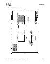
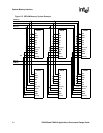
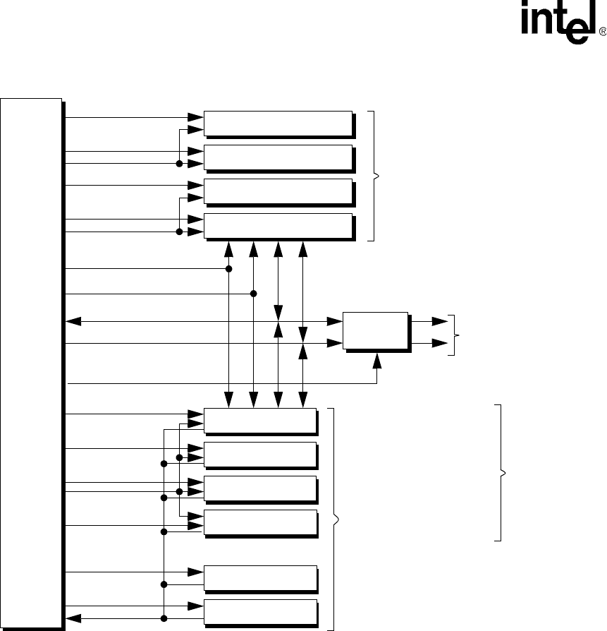
System Memory Interface
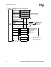
Figure 2-1. General Memory Interface Configuration
PXA250
Memory
Controller
Interface
SDRAM Partition 0
SDRAM Partition 1
SDRAM Partition 2
SDRAM Partition 3
nSDCS<0>
nSDCS<1>
nSDCS<2>
nSDCS<3>
nCS<0>
nCS<1>
nCS<2>
nCS<3>
nCS<4>
nCS<5>
Static Bank 3
Static Bank 4
Static Bank 5
Buffers and
Transceivers
DQM<3:0>
nSDRAS, nSDCAS
SDCLK<2>, SDCKE<1>
SDCLK<1>, SDCKE<1>
SDCLK<0>,
MD<31:0>
MA<25:0>
Card Control
RDY
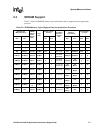
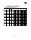
SDRAM Memory Interface
Up to 4 partitions of SDRAM
memory (16- or 32-bit wide)
Card Memory Interface
Up to 2-socket support.
Requires some
external buffering.
Synchronous Static Memory Interface
Up to 6 banks of ROM, Flash,
NOTE:
Static Bank 0 must be populated by
Static Memory or
Variable Latency I/O Interface
(16- or 32-bit wide)
(16- or 32-bit wide)
SRAM, Variable Latency I/O,
“bootable” memory
Static Bank 0
Static Bank 1
Static Bank 2
SDCKE<0>
Up to 4 banks of synchronous
static memory (nCS<3:0>).
NOTE:
Static Bank 0 must be populated by
“bootable” memory