


PXA250 and PXA210 Applications Processors Design Guide 8-17
Power and Clocking
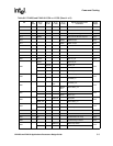
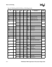
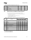
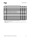
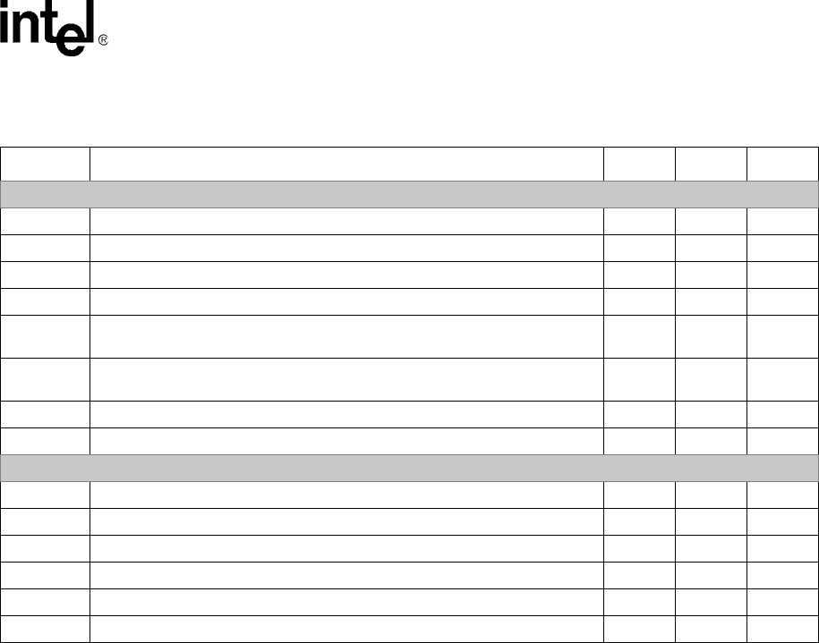
Table 8-14. Synchronous Memory Interface AC Specifications (3.3 V)
Symbol Description MIN MAX Notes
1
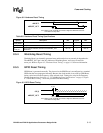
SDRAM / SMROM
tsynCLK SDCLK period 10 ns 20 ns 2
tsynCMD nSDCAS, nSDRAS, nWE, nSDCS assert time 1 sdclk — —
tsynRCD nSDRAS to nSDCAS assert time 1 sdclk — —
tsynCAS nSDCAS to nSDCAS assert time 2 sdclk — —
tsynSDOS
MA(25:0), MD(31:0), DQM(3:0), nSDCS(3:0), nSDRAS, nSDCAS, nWE, nOE,
SDCKE(1:0), RDnWR output setup time to SDCLK(2:0) rise
5ns — 3
tsynSDOH
MA(25:0), MD(31:0), DQM(3:0), nSDCS(3:0), nSDRAS, nSDCAS, nWE, nOE,
SDCKE(1:0), RDnWR output hold time from SDCLK(2:0) rise
5ns — 3
tsynSDIS MD(31:0) read data input setup time from SDCLK(2:0) rise 0.5 ns —
tsynDIH MD(31:0) read data input hold time from SDCLK(2:0) rise 1.5 ns — —
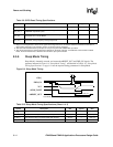
Fast Flash (Synchronous READS only)
tffCLK SDCLK period 15 ns 20 ns 4
tffAS MA(25:0) setup to nSDCAS (as nADV) asserted 0.5 sdclk — —
tffCES nCS setup to nSDCAS (as nADV) asserted 0.5 sdclk — —
tffADV nSDCAS (as nADV) pulse width 1 sdclk — —
tffOS nSDCAS (as nADV) deassertion to nOE assertion 3 sdclk — —
tffCEH nOE deassertion to nCS deassertion 4 sdclk — —
NOTES:
1. These numbers are for a maximum 99.5 MHz MEMCLK and 99.5 MHz output SDCLK.
2. SDCLK for SDRAM and SMROM can be at the slowest, divide-by-2 of the 99.5 MHz MEMCLK. It can be 99.5 MHz at the
fastest.
3. This number represents 1/2 SDCLK period.
4. SDCLK for Fast Flash can be at the slowest, divide-by-2 of the 99.5 MHz MEMCLK. It can be divide-by-2 of the 132.7 MHz
MEMCLK at its fastest.