


2-6 PXA250 and PXA210 Applications Processors Design Guide
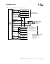
System Memory Interface
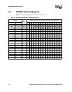
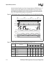
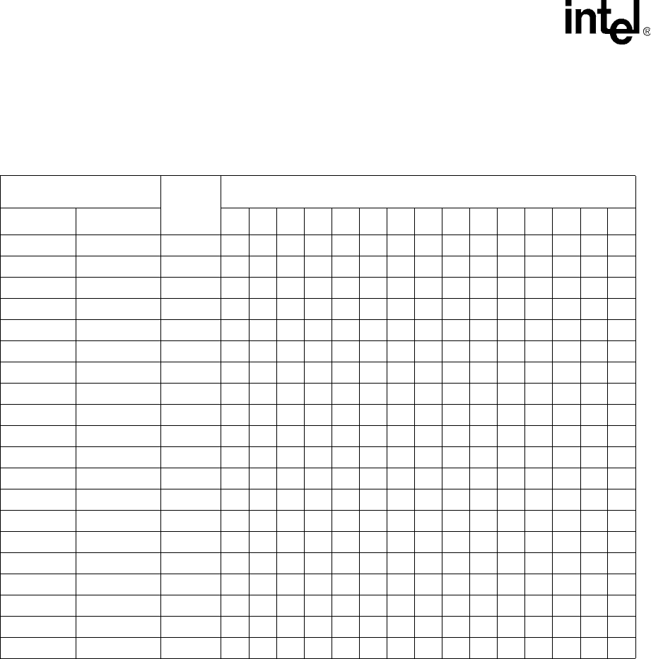
2.5 SDRAM Address Mapping
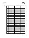
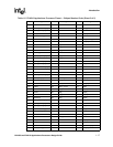
SDRAM Address Mapping is shown in Table 2-3 and Table 2-4.
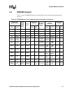
Table 2-3. Normal Mode Memory Address Mapping
SDRAM
# Bits
Bank x
Row x
Col
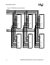
The applications processor pin mapping to SDRAM devices
(The address lines at the top of the columns are the processor address lines)
Device Technology
A24 A23 A22 A21 A20 A19 A18 A17 A16 A15 A14 A13 A12 A11 A10
1Mx16 16Mbit 1x11x8 BS0 A10 A9 A8 A7 A6 A5 A4 A3 A2 A1 A0
2Mx8 16Mbit 1x11x9 BS0 A10 A9 A8 A7 A6 A5 A4 A3 A2 A1 A0
4Mx4 16Mbit 1x11x10 BS0 A10 A9 A8 A7 A6 A5 A4 A3 A2 A1 A0
1x12x8 BS0A11A10A9A8A7A6A5A4A3A2A1A0
1x12x9 BS0A11A10A9A8A7A6A5A4A3A2A1A0
1x12x10 BS0A11A10A9A8A7A6A5A4A3A2A1A0
1x12x11 BS0A11A10A9A8A7A6A5A4A3A2A1A0
1x13x8 BS0 A12 A11 A10 A9 A8 A7 A6 A5 A4 A3 A2 A1 A0
1x13x9 BS0 A12 A11 A10 A9 A8 A7 A6 A5 A4 A3 A2 A1 A0
1x13x10 BS0 A12 A11 A10 A9 A8 A7 A6 A5 A4 A3 A2 A1 A0
1x13x11 BS0 A12 A11 A10 A9 A8 A7 A6 A5 A4 A3 A2 A1 A0
2Mx32 64Mbit 2x11x8 BS1BS0A10A9A8A7A6A5A4A3A2A1A0
2x11x9 BS1BS0A10A9A8A7A6A5A4A3A2A1A0
2x11x10 BS1BS0A10A9A8A7A6A5A4A3A2A1A0
4Mx16/4Mx32 64Mbit/128Mbit 2x12x8 BS1 BS0 A11 A10 A9 A8 A7 A6 A5 A4 A3 A2 A1 A0
8Mx8/8Mx16 64Mbit/128Mbit 2x12x9 BS1 BS0 A11 A10 A9 A8 A7 A6 A5 A4 A3 A2 A1 A0
16Mx4/16Mx8 64Mbit/128Mbit 2x12x10 BS1 BS0 A11 A10 A9 A8 A7 A6 A5 A4 A3 A2 A1 A0
32Mx4 128Mbit 2x12x11 BS1 BS0 A11 A10 A9 A8 A7 A6 A5 A4 A3 A2 A1 A0
8Mx32 256Mbit 2x13x8 BS1BS0A12A11A10A9A8A7A6A5A4A3A2A1A0
16Mx16 256Mbit 2x13x9 BS1BS1A12A11A10A9A8A7A6A5A4A3A2A1A0