


8-22 PXA250 and PXA210 Applications Processors Design Guide
Power and Clocking
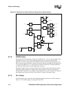
8.7.2 CORE Power
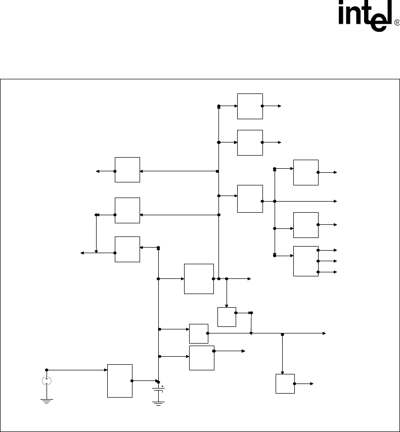
The example form factor reference design has a variable 0.8 V – 1.3 V core power supply for the
applications processor. This voltage varies depending on the performance required by the
application. A Linear Technologies LTC1878 buck converter is chosen for this application. The
power is drawn directly from the Li+ battery. This device operates at 550 kHz and can supply up to
1 A at 0.8 V and 800 mA at 1.3 V with up to 95% efficiency. The device is turned on/off by the
SA_PWR_EN signal directly from the applications processor.
The required output voltage is statically adjusted by selecting the value of the feed-back resistor.
Ultimately, output voltage can be changed using software control of the Linear Technologies
LTC1663 DAC. This DAC is controllable via the standard I2C bus, and can modify the voltage of
the feedback path of the buck converter, which effects a change in the output voltage.
8.7.3 PLL Power
DC_PLL supplies power to the three PLLs within the applications processor. This pin requires a
0.85 V to 1.3 V nominal supply at an expected 20 mA load.
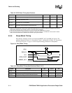
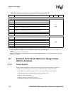
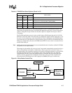
Figure 8-5. Example Form Factor Reference Design Power System Design
Boost
Converter
LTC1308A
Battery
Charger
LTC1730
Wall
Input
Current
Limited
battery
Buck
Converter
LTC1878
LDO
3.3 V
DC_CORE
LDO
ON/OFF
LDO
ON/OFF
Boost
Converter
MAX633
LDO
ON/OFF
LCD_DC15V
LCD_DC14V-
LCD_DC11P7V-
LCD_DC4V
LCD_DC5V
LCD_DC3P3V
DC_3P3V
DC_5P5V
LDO
ON/OFF
Audio_DC3P3V
LDO
ON/OFF
Audio AMP
LDO
ON/OFF
3.3V
CF_VDD
0.8 - 1.3 V
LDO
3.2 V
LDO
ON/OFF
3.2V
LDO
ON/OFF
3.3V
MMC_VDD
LDO
1.3 V
DC_PLL