


PXA250 and PXA210 Applications Processors Design Guide 7-1
I
2
C 7
The Inter-Integrated Circuit (I
2
C) bus interface unit lets the applications processor serve as a
master and slave device residing on the I
2
C bus. The I
2
C bus is a serial bus developed by Philips
Corporation consisting of a two-pin interface. SDA is the serial data line and SCL is the serial
clock line.
Using the I
2
C bus lets the applications processor interface to other I
2
C peripherals and
microcontrollers for system management functions. The serial bus requires a minimum of
hardware for an economical system to relay status and reliability information to an external device.
The I
2
C bus interface unit is a peripheral device that resides on the applications processor internal
bus. Data is transmitted to and received from the I
2
C bus via a buffered interface. Control and
status information is relayed through a set of memory-mapped registers. Refer to the I
2
C Bus
Specification for complete details on I
2
C bus operation.
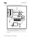
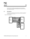
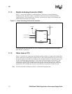
7.1 Schematics
The I
2
C bus is used by many different applications. This reference guide presents two possible
methods for using the I
2
C bus interface. The first method controls a digital-to-analog converter
(DAC) to vary the DC voltage to the processor core. The second method expands the capabilities of
an existing compact flash socket.
7.1.1 Signal Description
The I
2
C bus interface unit signals are SDA and SCL. Table 7-1 describes the function of each
signal.
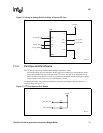
The I
2
C bus serial operation uses an open-drain, wired-AND bus structure, which allows multiple
devices to drive the bus lines and to communicate status about events such as arbitration, wait
states, error conditions and so on. For example, when a master drives the clock (SCL) line during a
data transfer, it transfers a bit on every instance that the clock is high. When the slave is unable to
accept or drive data at the rate that the master is requesting, the slave can hold the clock line low
between the high states to insert a wait interval. The master’s clock can only be altered by a slow
slave peripheral keeping the clock line low or by another master during arbitration.
The I
2
C bus lets you design a multi-master system; meaning more than one device can initiate data
transfers at the same time. To support this feature, the I
2
C bus arbitration relies on the wired-AND
connection of all I
2
C interfaces to the I
2
C bus. Two masters can drive the bus simultaneously
provided they are driving identical data. The first master to drive SDA high while another master
drives SDA low loses the arbitration. The SCL line consists of a synchronized combination of
clocks generated by the masters using the wired-AND connection to the SCL line.
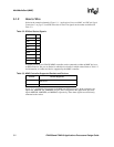
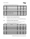
Table 7-1. I
2
C Signal Description
Signal Name Input/Output Description
SDA BiDirectional Serial data
SCL BiDirectional Serial clock