


PXA250 and PXA210 Applications Processors Design Guide 8-19
Power and Clocking
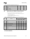
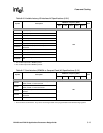
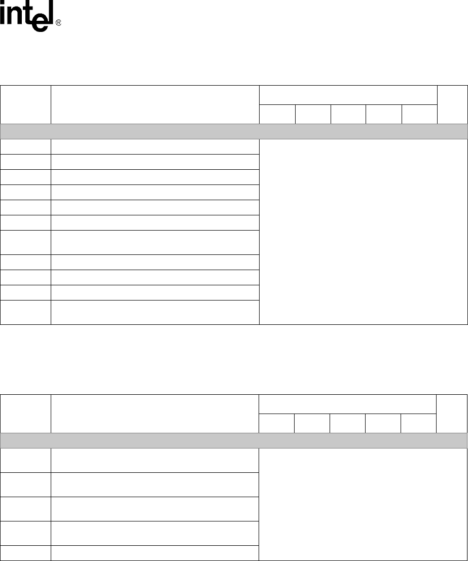
Table 8-16. Variable Latency I/O Interface AC Specifications (2.5 V)
Symbol Description
MEMCLK Frequency (MHz)
Notes
99.5 118.0 132.7 147.5 165.9
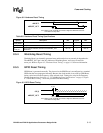
Variable Latency IO Interface (VLIO) (Asynchronous)
tvlioAS MA(25:0) setup to nCS asserted
TBD
tvlioASRW MA(25:0) setup to nOE or nPWE asserted
tvlioAH MA(25:0) hold after nOE or nPWE deasserted
tvlioCES nCS setup to nOE or nPWE asserted
tvlioCEH nCS hold after nOE or nPWE deasserted
tvlioDSW MD(31:0), DQM(3:0) write data setup to nPWE asserted
tvlioDSWH
MD(31:0), DQM(3:0) write data setup to nPWE
deasserted
tvlioDHW MD(31:0), DQM(3:0) hold after nPWE deasserted
tvlioDHR MD(31:0) read data hold after nOE deasserted
tvlioRDYH RDY hold after nOE, nPWE deasserted
tvlioNPWE
nPWE, nOE high time between beats of write or read
data
NOTES:
1. This number represents 1 MEMCLK period
2. This number represents 2 MEMCLK periods
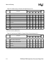
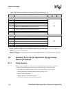
Table 8-17. Card Interface (PCMCIA or Compact Flash) AC Specifications (2.5 V)
Symbol Description
MEMCLK Frequency (MHz)
Notes
99.5 118.0 132.7 147.5 165.9
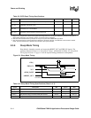
Card Interface (PCMCIA or Compact Flash) (Asynchronous)
tcardAS
MA(25:0), nPREG, PSKTSEL, nPCE setup to nPWE,
nPOE, nPIOW, or nPIOR asserted
TBD
tcardAH
MA(25:0), nPREG, PSKTSEL, nPCE hold after nPWE,
nPOE, nPIOW, or nPIOR deasserted
tcardDS
MD(31:0) setup to nPWE, nPOE, nPIOW, or nPIOR
asserted
tcardDH
MD(31:0) hold after nPWE, nPOE, nPIOW, or nPIOR
deasserted
tcardCMD nPWE, nPOE, nPIOW, or nPIOR command assertion
NOTE:
1. These numbers are minimums. They can be much longer based on the programmable Card Interface timing registers.