


3-8 PXA250 and PXA210 Applications Processor Design Guide
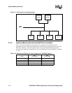
LCD Display Controller
3.5 Additional Design Considerations
3.5.1 Contrast Voltage
Many displays, both active and passive, include a pin for adjusting the display contrast voltage.
This is a variable analog voltage that is supplied to the panel via an voltage source on the system
board. The contrast voltage is adjusted via a variable resistor on the circuit board.
The required voltage range and current capabilities vary between panel manufacturers. Consult the
datasheet for your panel to determine the variable voltage circuit design. Ensure that the contrast
voltage is stable, otherwise visual artifacts might result. Possible contrast-voltage circuits are often
suggested by the panel manufacturers.
3.5.2 Backlight Inverter
One potential source of noise for the LCD panel can be the backlight inverter. Since this is a high
voltage device with frequent voltage inversions, it has the potential to inject spurious noise onto the
LCD panel lines. To minimize noise:
• Use a shielded backlight inverter
• Physically locate the inverter as far away from the LCD data lines and system board as
possible, usually located with the LCD panel
If power consumption is an issue, chose a backlight inverter that can be disabled through software.
This lets you save power by automatically disabling the backlight if no activity occurs within a
preset period of time
3.5.3 Signal Routing and Buffering
Signal transmission rates between the LCD controller and the LCD panel are moderate, which
helps to simplify the design of the LCD system. The minimum Pixel Clock Divider (PCD) value
results in a pixel clock rate of one half of the LCLK (this is not the L_LCLK of the LCD
controller.) The maximum LCLK for the PXA250 applications processor is 166 MHz, resulting in
a maximum pixel clock rate of 83 MHz. Thus, use of 100 MHz design considerations are sufficient
to ensure LCD panel signal integrity.
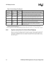
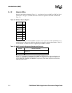
L_DD12 A3
L_DD13 A2
L_DD14 C3
L_DD15 B3
L_FCLK E8
L_LCLK D8
L_PCLK B8
Bias A8
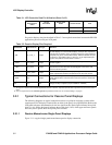
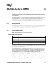
Table 3-4. PXA250 LCD Controller Ball Positions (Sheet 2 of 2)
Pin Name Ball Position