


1-10 PXA250 and PXA210 Applications Processors Design Guide
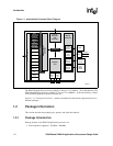
Introduction
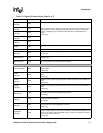
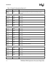
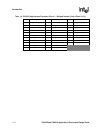
VSSN SUP
Ground supply for memory bus and PCMCIA pins. Connect these pins to the common
ground plane on the PCB.
BATT_VCC SUP
Backup battery connection. Connect this pin to the backup battery supply. If a backup
battery is not required then this pin may be connected to the common 3.3v supply on
the PCB.
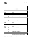
NOTES:
1. Not pinned out for the PXA210 applications processor.
2. GPIO Reset Operation: After any reset, these pins are configured as GPIO inputs by default. The input buffers for these pins
are disabled to prevent current drain and must be enabled prior to use by clearing the Read Disable Hold (RDH) bit.
To use a GPIO pin as an alternate function, follow this sequence:
1) Program the pin to the desired direction (input or output) using the GPIO Pin Direction Registers (GPDR).
2) Enable the input buffer by clearing the RDH bit, described above.
3) If needed, select the desired alternate function by programming the proper bits in the GPIO Alternate Function
Register (GAFR).
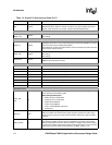
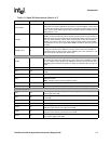
Table 1-3. Signal Pin Descriptions (Sheet 7 of 7)
Name Type Description