


8-2 PXA250 and PXA210 Applications Processors Design Guide
Power and Clocking
8.2 Electrical Specifications
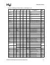
Table 8-2 provides the Absolute Maximum ratings for the applications processor. These parameters
may not be exceeded or the part may be permanently damaged. Operation at Absolute Maximum
Ratings is not guaranteed.
8.3 Power Consumption Specifications
Power consumption on any highly integrated device is extremely dependent on the operating
voltage, external switching activity, and external loading (shown in Table 8-3, “Power
Consumption Specifications” on page 8-3). Because power consumption on the applications
processor is optimized, power varies based on which functions are being performed and by the data
and frequency requirements of the module.
The maximum power consumption specification is determined by all units running at their
maximum: processor speed, voltage, and loading conditions. This method generates a conservative
power consumption value; however, power supply and thermal management design requires the
highest possible power consumption for robust design.The applications processor’s maximum
power consumption is calculated using the following conditions:
• All peripheral units operating at maximum frequency and size configuration
• All I/O loads maximum (50pF for Memory interface, 100pF for peripherals)
• Core operating at worst case power scenario (hit rates adjusted for worst power)
• All voltages at maximum of range
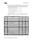
Table 8-2. Absolute Maximum Ratings
Symbol Description Min Max
T
S
Storage Temperature -40° C 125° C
V
SS_O
Offset Voltage between any two VSS pins
(VSS, VSSQ, VSSN)
-0.3 V 0.3 V
V
CC_O
Offset Voltage between any of the following pins:
VCCQ, VCCN
-0.3 V 0.3 V
V
CC_HV
Voltage Applied to High Voltage Supplies
(VCCQ, VCCN)
VSS-0.3 V VSS+4.0 V
V
CC_LV
Voltage Applied to Low Voltage Supplies
(VCC, PLL_VCC)
VSS-0.3 V VSS+1.45 V
V
IP
Voltage Applied to non-Supply pins except XTAL pins VSS-0.3 V
max of
VCCQ+0.3 V,
VSS+4.0 V
V
IP_X
Voltage Applied to XTAL pins
(PXTAL, PEXTAL, TXTAL, TEXTAL)
VSS-0.3 V
max of
VCC+0.3 V,
VSS+1.45 V
V
ESD
Maximum ESD stress voltage, Human Body Model;
Any pin to any supply pin, either polarity, or
Any pin to all non-supply pins together, either polarity.
Three stresses maximum.
2000 V
I
EOS
Maximum DC Input Current (Electrical Overstress) for any non-supply pin 5mA