


9-2 PXA250 and PXA210 Applications Processors Design Guide
JTAG/Debug Port
9.3 Layout
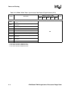
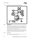
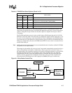
Use the JTAG/Debug the port layout recommendations given in ARM’s application note, Multi-
ICE System Design Considerations, Application Note 72. The recommended connector is a 2x10-
way, 2.54 mm pitch pin header, shown in Figure 9-1.
If board space is critical, use a small form-factor receptacle with a smaller pitch. Then use a cable
interface that has a wire “dongle” with a 2.54 mm pitch pin header on one end and the smaller pitch
connector on the other.
Place the JTAG/Debug connector as close as possible to the applications processor to minimize
signal degradation.
If you follow these design recommendations, a JTAG bridge board is not required. Essentially, the
JTAG bridge board for the example form factor reference design uses a 220 ohm resistor to tie
nTRST high so that the JTAG logic can be brought out of reset (otherwise it would not come out of
reset since nTRST is open-drain).