


1-4 PXA250 and PXA210 Applications Processors Design Guide
Introduction
• I
2
C Controller pins
• PWM pins
• 2 dedicated GPIOs pins
• Integrated JTAG support
1.2.2 Signal Pin Descriptions
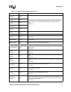
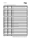
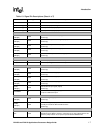
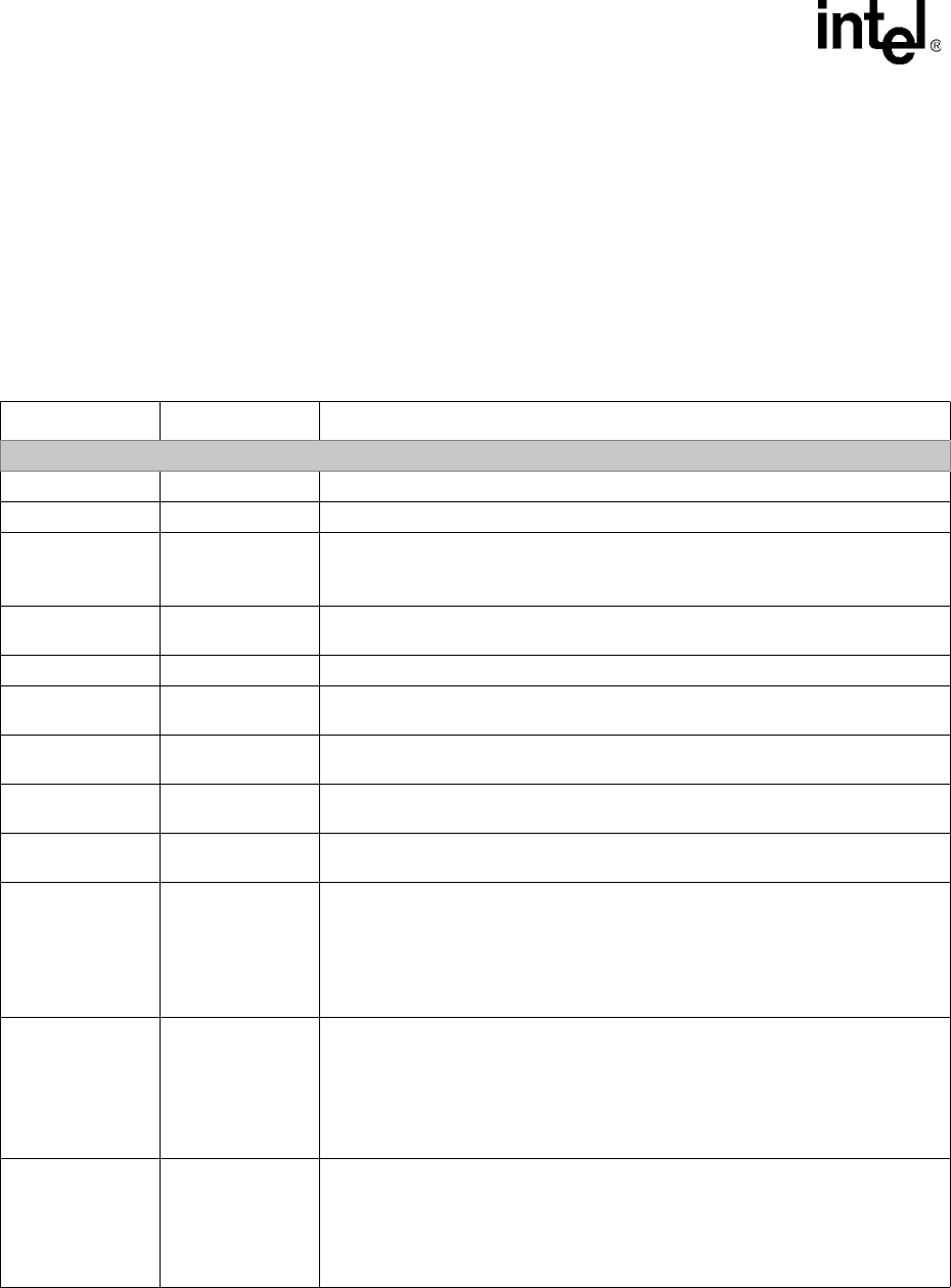
Table 1-3 defines the signal descriptions for the applications processor.
Table 1-3. Signal Pin Descriptions (Sheet 1 of 7)
Name Type Description
Memory Controller Pins
MA[25:0] OCZ Memory address bus. This bus signals the address requested for memory accesses.
MD[15:0] ICOCZ Memory data bus. D[15:0] are used for 16-bit and 32-bit data modes.
MD[31:16] ICOCZ
Memory data bus. D[31:16]: These signals are the upper memory data bus address
bits.
See Note [1]
nOE OCZ
Memory output enable. Connect this signal to the output enables of memory devices
to control their data bus drivers.
nWE OCZ Memory write enable. Connect this signal to the write enables of memory devices.
nSDCS[3:0] OCZ
SDRAM CS for banks 0 through 3. Connect these signals to the chip select (CS) pins
for SDRAM. nSDCS0 is a three-state signal, while nSDCS1-3 are not three-state.
DQM[3:0] OCZ
SDRAM DQM for data bytes 0 through 3. Connect these signals to the data output
mask enables (DQM) for SDRAM.
nSDRAS OCZ
SDRAM RAS. Connect this signal to the row address strobe (RAS) pins for all banks
of SDRAM.
nSDCAS OCZ
SDRAM CAS. Connect this signal to the column address strobe (CAS) pins for all
banks of SDRAM.
SDCKE[0] OC
SDRAM and/or Synchronous Static Memory/SDRAM-like synchronous Flash clock
enable clock enable.
ConnectSDCKE[0] to the CKE pins of SMROM and SDRAM-timing Synchronous
Flash.
The memory controller provides control register bits for deassertion of each SDCKE
pin.
SDCKE[1] OC
SDRAM device clock enable.
Connect SDCKE[1] to the clock enable pins of SDRAM. It is de-asserted (held low)
during sleep. SDCKE[1] is always deasserted upon reset.
The memory controller provides control register bits for deassertion of each SDCKE
pin.
See Note [1]
SDCLK[2:0] OCZ
Use these clocks to clock synchronous memory devices:
SDCLK0 - connected to either SMROM or synchronous Flash devices
SDCLK1 - connected to SDRAM banks 0/1
SDCLK2 - connected to SDRAM banks 2/3
See Note [1]