PXA250 and PXA210 Applications Processors Design Guide 2-9
System Memory Interface
2.6.3 SRAM / ROM / Flash / Synchronous Fast Flash Memory
Options
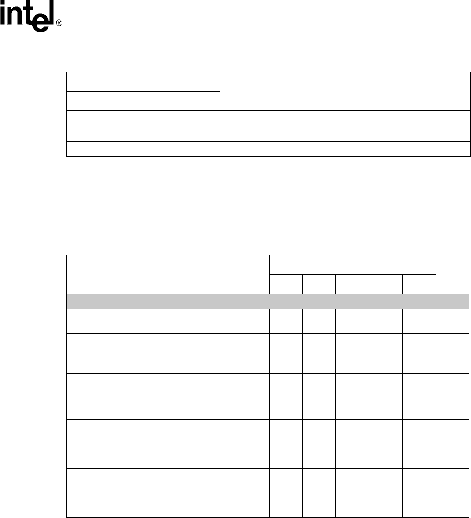
Table 2-7 contains the AC specification for SRAM / ROM / Flash / Synchronous Fast Flash.
2.6.4 Variable Latency I/O Interface Overview
Both reads and writes for VLIO differ from SRAM in that the PXA250 applications processor
samples the data-ready input, RDY. The RDY signal is level sensitive and goes through a two-stage
synchronizer on input. When the internal RDY signal is high, the I/O device is ready for data
transfer. This means that for a transaction to complete at the minimum assertion time for either
nOE or nPWE (RDF+1), the RDY signal must be high two clocks prior to the minimum assertion
time for either nOE or nPWE (RDF-1). Data will be latched on the rising edge of memclk once the
internal RDY signal is high and the minimum assertion time of RDF+1 has been reached. Once the
1 0 1 1 16-bit Synchronous Mask ROM (64 Mbits)
1 1 0 2 16-bit Synchronous Mask ROMs = 32-bits (64 Mbits each)
1 1 1 1 16-bit Synchronous Mask ROM (64 Mbits)
Table 2-6. BOOT_SEL Definitions (Sheet 2 of 2)
BOOT_SEL
Boot From . . .
210
Table 2-7. SRAM / ROM / Flash / Synchronous Fast Flash AC Specifications
Symbol Description
MEMCKLK
Units
Notes
99.5 118.0 132.7 147.5 165.9
SRAM / ROM / Flash / Synchronous Fast Flash (WRITES) (Asynchronous)
tromAS
MA(25:0) setup to nOE, nSDCAS (as
nADV) asserted
10 8.5 7.5 6.8 6 ns, 1
tromAH
MA(25:0) hold after nCS, nOE,
nSDCAS (as nADV) de-asserted
10 8.5 7.5 6.8 6 ns, 1
tromASW MA(25:0) setup to nWE asserted 30 25.5 22.5 20.4 18 ns, 3
tromAHW MA(25:0) hold after nWE de-asserted 10 8.5 7.5 6.8 6 ns, 1
tromCES nCS setup to nWE asserted 20 17 15 13.6 12 ns, 2
tromCEH nCS hold after nWE de-asserted 10 8.5 7.5 6.8 6 ns, 1
tromDS
MD(31:0), DQM(3:0) write data setup to
nWE asserted
10 8.5 7.5 6.8 6 ns, 1
tromDSWH
MD(31:0), DQM(3:0) write data setup to
nWE de-asserted
20 17 15 13.6 12 ns, 2
tromDH
MD(31:0), DQM(3:0) write data hold
after nWE de-asserted
10 8.5 7.5 6.8 6 ns, 1
tromNWE
nWE high time between beats of write
data
20 17 15 13.6 12 ns, 2
NOTES:
1. This number represents 1 MEMCLK period
2. This number represents 2 MEMCLK periods


