


PXA250 and PXA210 Applications Processors Design Guide 8-15
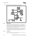
Power and Clocking
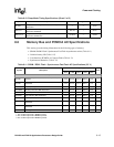
8.6 Memory Bus and PCMCIA AC Specifications
This section gives the timing information for the following types of memory:
• SRAM / ROM / Flash / Synchronous Fast Flash Asynchronous writes (Table 8-11)
• Variable Latency I/O (Table 8-12)
• Card Interface (PCMCIA or Compact Flash) (Table 8-13)
• Synchronous Memories (Table 8-14)
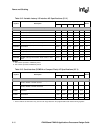
t
D_FAULT
Delay between PWR_EN asserted and nVDD_FAULT
deasserted
— — 10 ms
t
DSM_OUT
Delay between PWR_EN asserted and nRESET_OUT
deasserted, OPDE Set
28.0 ms — 80 ms
t
DSM_OUT_O
Delay between PWR_EN asserted and nRESET_OUT
deasserted, OPDE Clear
10.35 ms — 10.5 ms
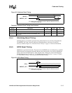
Table 8-10. Sleep Mode Timing Specifications (Sheet 2 of 2)
Symbol Description Min Typical Max
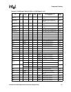
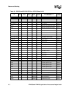
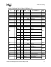
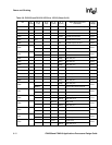
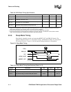
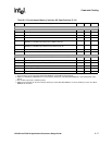
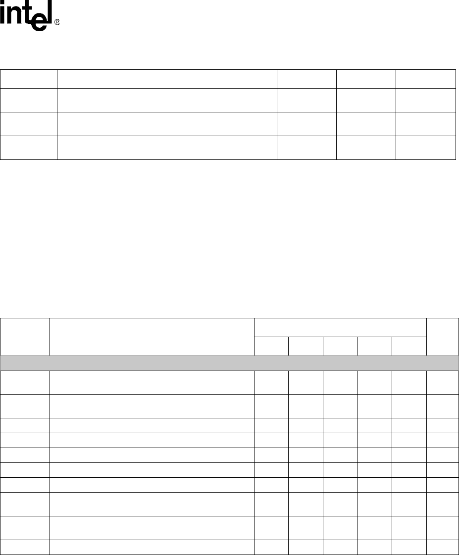
Table 8-11. SRAM / ROM / Flash / Synchronous Fast Flash AC Specifications (3.3 V)
Symbol Description
MEMCLK Frequency (MHz)
Notes
99.5 118.0 132.7 147.5 165.9
SRAM / ROM / Flash / Synchronous Fast Flash (WRITES) (Asynchronous)
tromAS
MA(25:0) setup to nCS, nOE, nSDCAS (as nADV)
asserted
10 ns 8.5 ns 7.5 ns 6.8 ns 6 ns 1
tromAH
MA(25:0) hold after nCS, nOE, nSDCAS (as nADV)
deasserted
10 ns 8.5 ns 7.5 ns 6.8 ns 6 ns 1
tromASW MA(25:0) setup to nWE asserted 30 ns 25.5 ns 22.5 ns 20.4 ns 18 ns 2
tromAHW MA(25:0) hold after nWE deasserted 10 ns 8.5 ns 7.5 ns 6.8 ns 6 ns 1
tromCES nCS setup to nWE asserted 20 ns 17 ns 15 ns 13.6 ns 12 ns 3
tromCEH nCS hold after nWE deasserted 10 ns 8.5 ns 7.5 ns 6.8 ns 6 ns 1
tromDS MD(31:0), DQM(3:0) write data setup to nWE asserted 10 ns 8.5 ns 7.5 ns 6.8 ns 6 ns 1
tromDSWH
MD(31:0), DQM(3:0) write data setup to nWE
deasserted
20 ns 17 ns 15 ns 13.6 ns 12 ns 3
tromDH
MD(31:0), DQM(3:0) write data hold after nWE
deasserted
10 ns 8.5 ns 7.5 ns 6.8 ns 6 ns 1
tromNWE nWE high time between beats of write data 20 ns 17 ns 15 ns 13.6 ns 12 ns 3
NOTES:
1. This number represents 1 MEMCLK period
2. This number represents 3 MEMCLK periods
3. This number represents 2 MEMCLK periods