


2-10 PXA250 and PXA210 Applications Processors Design Guide
System Memory Interface
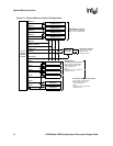
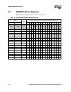
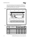
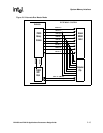
data has been latched, the address may change on the next rising edge of MEMCLK or any cycles
thereafter. The nOE or nPWE signal de-asserts one MEMCLK after data is latched. Before a
subsequent data beat, nOE or nPWE remains deasserted for RDN+1 memory cycles. The chip
select and byte selects, DQM[3:0], remain asserted for one memory cycle after the burst’s final
nOE or nPWE deassertion. Refer to
Figure 2-3 for 32-Bit Variable Latency I/O read timing and
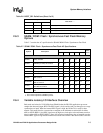
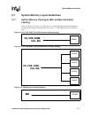
Figure 2-8 for Variable Latency I/O Interface AC Specifications
Figure 2-3. 32-Bit Variable Latency I/O Read Timing (Burst-of-Four, One Wait Cycle Per Beat)
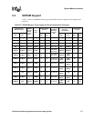
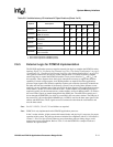
Table 2-8. Variable Latency I/O Interface AC Specifications (Sheet 1 of 2)
Symbol Description
MEMCKLK
Units
Notes
99.5 118.0 132.7 147.5 165.9
Variable Latency IO Interface (VLIO) (Asynchronous)
tvlioAS MA(25:0) setup to nCS asserted 10 8.5 7.5 6.8 6 ns, 1
tvlioASRW
MA(25:0) setup to nOE or nPWE
asserted
10 8.5 7.5 6.8 6 ns, 1
tvlioAH
MA(25:0) hold after nOE or nPWE de-
asserted
10 8.5 7.5 6.8 6 ns, 1
tvlioCES nCS setup to nOE or nPWE asserted 20 17 15 13.6 12 ns, 2
tvlioCEH
nCS hold after nOE or nPWE de-
asserted
10 8.5 7.5 6.8 6 ns, 1
A8867-01
"0000"
"00"
012 3
nCS[1]
DQM[3:0]
MD[31:0]
RDY
RDnWR
nPWE
nOE
MA[25:2]
MA[1:0]
nCS[0]
memlk
0ns 100ns 200ns 300ns
tCES RDN+1
tASWN
tCEH
RRR+1
RDF+1+Waits
tAS
tAH
tASRW0