


7-2 PXA250 and PXA210 Applications Processors Design Guide
I2C
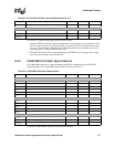
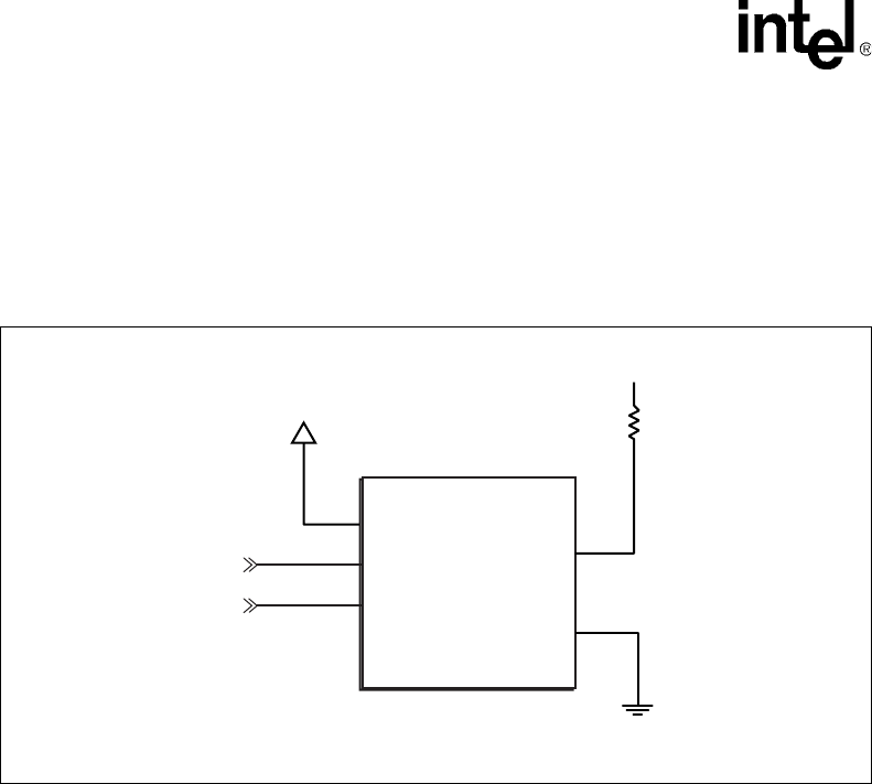
7.1.2 Digital-to-Analog Converter (DAC)
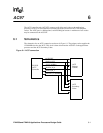
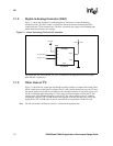
Figure 7-1 shows the schematic for connecting the I
2
C interface to a Linear Technology
micropower DAC. The DAC output is connected to the buck converter feedback path and is
controlled by the I
2
C bus interface unit. The DAC can modify the voltage of the feedback path,
which effects the processor core voltage.
The signals SA_I2C_SDA and SA_I2C_SCL correspond to the applications processor signals
SDA and SCL, respectively.
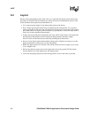
7.1.3 Other Uses of I
2
C
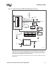
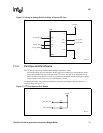
Figure 7-2 shows the I
2
C signals passing through an analog switch to a compact flash socket. Since
the CF socket has all of the signals to support two CF cards, and this design only uses one CF card,
the signals meant for a second card are being used for alternate functions. If you decide not to use a
CF card, a different application using a CF card socket could be designed to utilize the I
2
C bus
interface unit. If this alternate function is used, the I
2
C bus can be enabled to the CF socket by
asserting the signal SA_I2C_ENAB shown in the diagram. If the user decides to use a CF Card,
negate the SA_I2C_ENAB signal so the I
2
C bus traffic does not interfere with the CF card.
Note: The CF card socket is disabled if a device is inserted in the expansion bus.
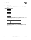
Figure 7-1. Linear Technology DAC with I
2
C Interface
A8752-01
LTC1663C35
DC3P3V
R165 1.00M
LTC1663
U30
LTEP
VCC
VOUT
GND
3
2
SA_I2C_SDA
SDA
1
4
SA_I2C_SCL
SCL
5