


3-6 PXA250 and PXA210 Applications Processor Design Guide
LCD Display Controller
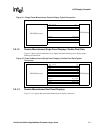
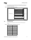
3.3.1 Typical connections for Active Panel Displays
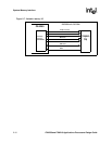
Figure 3-6, “Active Color Display Typical Connection” on page 7 shows a typical connection for
an active panel display and should serve as a guide for designing systems which contain active
LCD displays. The MSB of each color is indicated. The panel is 18-bit, with the LSB of red and
blue tied to ground.
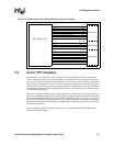
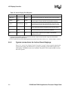
Table 3-3. Active Display Pins Required
PXA250 Pin LCD Panel Pin PIn Type
1
Definition
L_DD<15:0>
R<4:0>,G<5:0>,
B<4:0>
Output Data lines used to transmit the 16 bit data values to the LCD display.
L_PCLK Clock Output
Pixel Clock - used by the LCD display to clock the pixel data into the
line shift register. In active mode this clock transitions constantly.
L_LCLK Horizontal Sync Output
Line Clock - used by the LCD display to signal the end of a line of pixels
that transfers the line data from the shift register to the screen and
increment the line pointers. Also signals the panel to start a new line.
L_FCLK Vertical Sync Output
Frame Clock - used by the LCD displays to signal the start of a new
frame of pixels that resets the line pointers to the top of the screen.
L_BIAS
DE (Data
Enable)
Output
AC biases used in active mode as a data enable signal when data
should be latched by the pixel clock from the data lines.
N/A Vcon
2
N/A
Contrast Voltage - Adjustable voltage input to LCD panel - external
voltage circuitry is required (no pin available on the PXA250
applications processor).
NOTES:
1. In reference to
the PXA250 applications processor. Therefore, outputs are pins that drive a signal from the PXA250
applications processor to another device.
2. Vcon is a signal external to
the PXA250 applications processor. Please refer to Section 3.5.1, “Contrast Voltage” on page 8.