


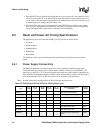
PXA250 and PXA210 Applications Processors Design Guide 8-1
Power and Clocking 8
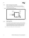
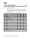
8.1 Operating Conditions
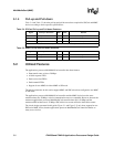
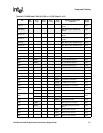
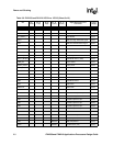
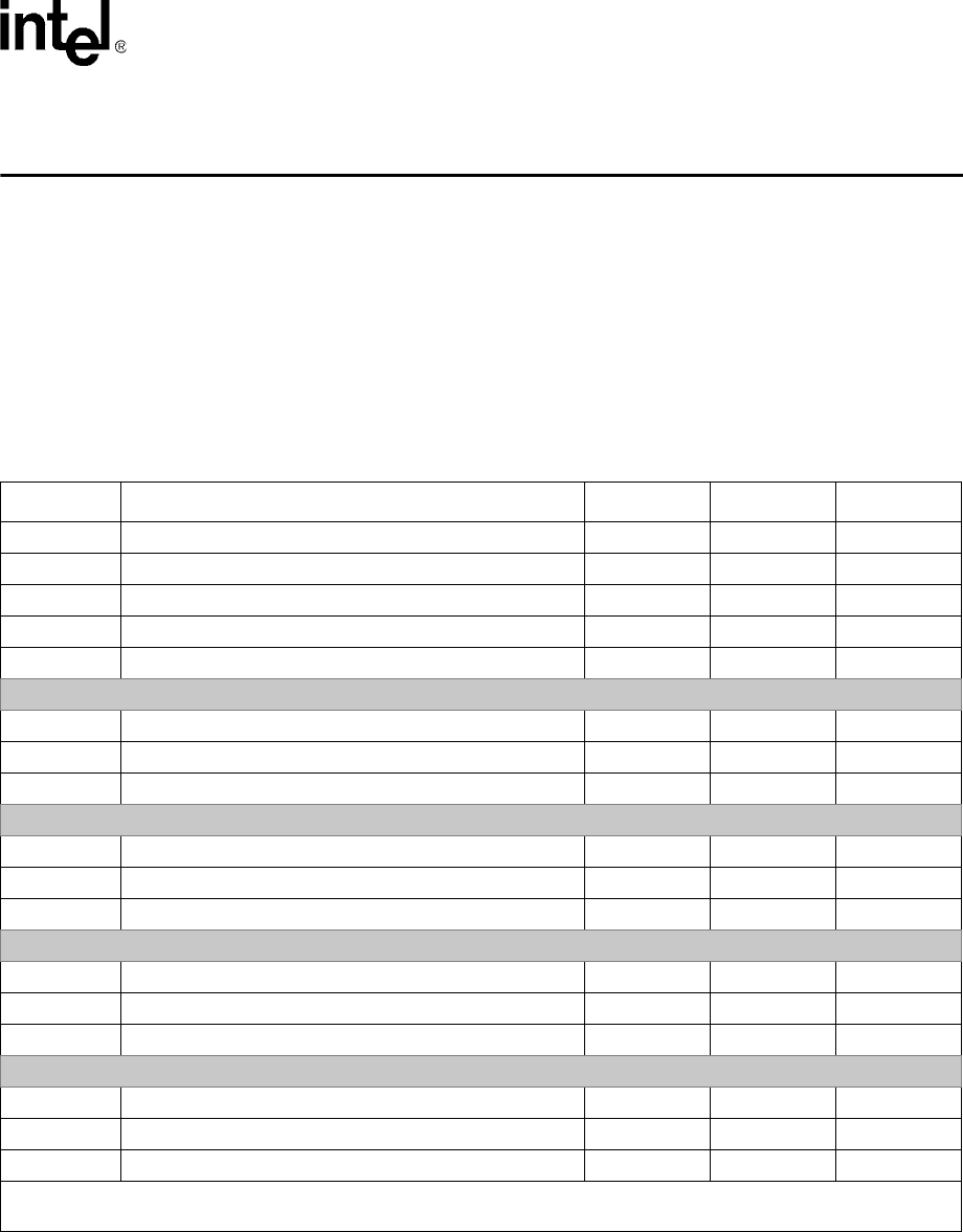
Table 8-1 shows voltage, frequency, and temperature specifications for the applications processor
for four different ranges. The temperature specification for each range is constant; the frequency
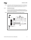
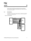
range is operation voltage dependent. On a prototype design, the VCC/PLL_VCC regulator should
have a range from 0.85 V to 1.65 V. PLL_VCC and VCC must be connected together on the board
or driven by the same supply.
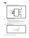
Table 8-1. Voltage, Temperature, and Frequency Electrical Specifications
Symbol Description Min Typical Max
t
A
Ambient Temperature -40°C — 85° C
V
VSS
VSS, VSSN, VSSQ Voltage -0.3 V 0V 0.3 V
V
VCCQ
VCCQ 3.0 V 3.3 V 3.6 V
V
VCCN_H
VCCN @ 3.3V 3.0 V 3.3 V 3.6 V
V
VCCN_L
VCCN @ 2.5V 2.375 V 2.5 V 2.625 V
Low Voltage Range (PXA210 and PXA250)
V
VCC_L
VCC, PLL_VCC Voltage, Low Range 0.8075 V 0.85 V 0.935 V
f
TURBO_L
Turbo Mode Frequency, Low Range 99.5 MHz — 132.7 MHz
f
SDRAM_L
External Synchronous Memory Frequency, Low Range — — 66.4 MHz
Medium Voltage Range (PXA250 and PXA210)
V
VCC_M
VCC, PLL_VCC Voltage, Mid Range 0.9 V 1.0 V 1.1 V
f
TURBO_M
Turbo Mode Frequency, Mid Range 99.5 MHz — 199.1 MHz
f
SDRAM_M
External Synchronous Memory Frequency, Mid Range — — 99.5 MHz
High Voltage Range (PXA250 applications processor only)
V
VCC_H
VCC, PLL_VCC Voltage, High Range 1.0 V 1.1 V 1.21 V
f
TURBO_H
Turbo Mode Frequency, High Range 99.5 MHz — 298.7 MHz
f
SDRAM_H
External Synchronous Memory Frequency, High Range — — 99.5 MHz
Peak Voltage Range (PXA250 applications processor only)
V
VCC_P
VCC, PLL_VCC Voltage, Peak Range 1.17 V 1.3 V 1.43 V
f
TURBO_P
Turbo Mode Frequency, Peak Range 99.5 MHz — 398.2 MHz
f
SDRAM_P
External Synchronous Memory Frequency, Peak Range — — 99.5 MHz
NOTE: When VCCN=2.5 V, the I/O signals that are supplied by VCCN are 2.5 V tolerant only. Do not apply 3.3 V to any pin
supplied by VCCN in this case.