


164
Chapter 8: Theory of Operation
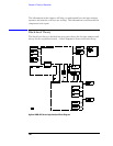
Agilent 1680A,AD-series Logic Analyzer Theory
resent via DMA transactions to an IEEE 1394 Link Layer chip. The Link Layer
then transmits the data to a 1394 PHY (physical layer chip) where the data is
transmitted over a 1394 cable to the motherboard for processing.
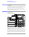
Test and Clock Synchronization Circuit. ECLinPS (ECL in pico seconds) ICs
are used in the Test and Clock Synchronization Circuit for reliability and low
channel-to-channel skew. Test patterns are generated and sent to the
comparators during software operation verification (self-tests). The test
patterns are propagated across all data and clock channels and read by the
acquisition ICs to verify that the data and clock pipelines are operating correctly.
Clock and Data Threshold. The threshold circuit includes a precision octal
DAC. Each of the eight channels of the DAC is individually programmable which
allows the user to set the thresholds of the individual pods. The 16 data channels
and the clock/data channel of each pod are all set to the same threshold voltage.
Motherboard Interface. The motherboard communications to the acquisition
board over an IEEE 1394 interface residing on the acquisition board. Changes to
the logic analyzer configuration made in application software are translated into
configuration commands and then sent to the acquisition board through this
interface. All state and timing functions including storage qualification,
sequencing, assigning clocks and qualifiers, RUN and STOP, and thresholds are
controlled in the manner.
A microcontroller manages initialization of the acquisition board at power-up,
reconfiguring the acquisition board as a result of user input, and managing the
IEEE 1394 communication to and from the motherboard.
A field programmable gate array (FPGA) bridges the 1394 interface to the rest of
the acquisition board components. It also serves as the memory controller for the
acquisition memory.
Memory Address Counters (MACs). Each acquisition IC has a CPLD that is
used to provide addresses to the memory ICs that are written during an
acquisition. The MACs are also used when uploading data to the GUI. Each CPLD
contains three MACs. The MACs are configured serially by the FPGA prior to
each acquisition and prior to each data upload. The application is responsible for
setting up the proper address by writing to various register in the FPGA, which
results in the MACs being serially programmed by the FPGA.
+5 VDC supply. The +5 VDC supply circuit supplies power to active logic
analyzer accessories such as analysis probes. Thermistors on the +5 VDC supply
lines protect the logic analyzer and the active accessory from overcurrent
conditions. When an overcurrent condition is sensed, the thermistors create an
open that shuts off the current rom the +5 VDC supply. After the overcurrent
condition is resolved the thermistor closes the circuit and makes the supply
current available.