


163
Chapter 8: Theory of Operation
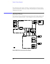
Agilent 1680A,AD-series Logic Analyzer Theory
The probe tip networks are comprised of a series of resistors (250 Ohm)
connected to a parallel combination of a 90 KOhm resistor and an 8.5 pF
capacitor. The parallel 90 KOhm and 8.5 pF capacitor along with the glossy cable
and terminations form a divide-by Ohm tip resistor is used to buffer (or raise the
impendence of) the 8.5 pF capacitor that is in series with the cable capacitance.
Comparators. Two 9-channel comparators interpret the incoming data and
clock signals as either high or low, depending on where the user-programmable
threshold is set. The threshold voltage of each pod is individually programmed,
and the voltage selected applies to the clock channel as well as the data channels
of each pod.
Each of the comparators has a serial test input port used for testing purposes. A
test bit pattern is sent from the Test and Clock Synchronization Circuit to the
comparator. The comparators then propagate the test signal on each of the nine
channels of the comparator. Consequently, the operating system software can
test all data and clock channel pipelines on the circuit board through the
comparator.
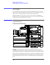
Acquisition. Each acquisition circuit is made up of a single acquisition circuit.
Each acquisition is a 34-channel state/timing analyzer. One to four acquisition ICs
are included on each logic analyzer board for a total of up to 128 data channels
and four state clock (pods one through four) in state mode. There are 136 data
channels available in timing mode. All of the sequencing, store qualification,
pattern/range recognition and event counting functions are performed by the
acquisition IC.
Additionally, the acquisition ICs perform master clocking functions. All four state
acquisition clocks are sent to the first two acquisition ICs, and the acquisition ICs
generate their own sample clocks. When necessary, the acquisition ICs
individually perform a clock optimization after the user selects the RUN icon and
before data is stored.
Clock optimization involves using programmable delays in the acquisition ICs to
position the master clock transition where valid data is captured. This procedure
greatly reduces the effects of channel-to-channel skew and other propagation
delays.
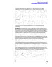
In the timing acquisition mode, an oscillator-driven clock circuit provides a 100
MHz clock signal to each of the acquisition IPs where they are multiplied by a PLL
to obtain the necessary internal clock frequency. For high speed timing
acquisition, the master acquisition IC derives the sampling frequency using its
PLL and redistributes this sampling clock to the other acquisition ICs.
Acquisition RAM. The acquisition RAM is external to the acquisition IC. The
acquisition RAM consists of 9 RAM ICs per acquisition chip. A CPLD, which is
initialized by the FPGA, increments the memory addresses while reading or
writing to the memory. Memory is read to the FPGA where it is translated and