


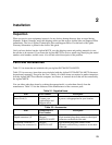

Installation - 2
31
1. Multiply the power generated by one cell times the number of cells in the Agilent MCCD. Divide the
result by the efficiency of the unit to determine the total output power produced by that mainframe.
The efficiency of the unit in discharging mode is assumed to be 100% which is a worst-case value as
far as calculating the total power that is generated by the mainframe.
#_of_cells × power_per_cell
1.0
= Max_power_out
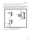
2. Divide the power generated by the Agilent MCCD by the input voltage of the Agilent Powerbus
Load. At an input voltage of 26.5 volts, the result will be the maximum discharging current that will
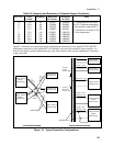
be absorbed by the Agilent Powerbus Load. (Double this current if you are simultaneously
discharging two Agilent MCCD mainframes as illustrated in Figure 2-5.)
Max_ power_out
26.5
= Max_powerbus_current
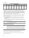
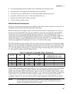
3. Determine the voltage drop that the maximum current will produce in the power bus leads using the
resistance values in Table 2-6.
4. The sum of the voltage drops in both the + and
−
power bus leads cannot exceed 1.5V. If the
voltage drop exceeds 1.5 volts in discharging mode, the Agilent MCCD will shut down due to an
overvoltage condition at the mainframe terminals. Use a larger size wire to reduce the voltage drop.
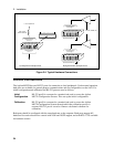
Digital Connections
Each Agilent E4370A MCCD mainframe has a 16-bit digital I/O port. Digital I/O configuration can be
done with the Agilent MCCD Configuration Screens as described in chapter 3 or with the Agilent MCCD
User Interface as described in chapter 4. All pins do not have to be configured the same. Some can be
used as isolated outputs while others are single ended I/O. The functions can also be mixed, some pins
can be general purpose I/O while others have a specific purpose. The polarity of a bit can also be
configured as either high true or low true. The following list documents the types of digital I/O
configurations:
General Purpose I/O
General purpose I/O programs the digital I/O as a passthrough function that allow input or output signals
on the digital connector to be directly controlled with API programming commands. These signals have
no effect on the cell forming sequence.
Digital Output
When configured as outputs, each line is driven by an internal open collector
transistor. Output lines are capable of driving either TTL compatible inputs, or high
power loads such as solenoids, indicator lights, and relays. These are 24 V/ 300mA
compatible open-collector outputs.
Digital Input
When configured as inputs, each line can be driven by an external source. All lines
are TTL compatible inputs, with built in pull-ups to 5 V to facilitate contact and
switch closure style inputs.
Digital InOut
When configured as in/out, each line can be used as both an input and an output.
Programming the line high allows an external device to drive the line. Programming
the line low drives the line low. Reading the line returns the actual state of the line.