


Register-Level Programming Appendix C
PC-OPDIO-16 User Manual C-2 © National Instruments Corporation
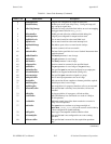
Register Description
Register Description Format
The remainder of this chapter discusses each of the PC-OPDIO-16 registers in the order shown
in Table C-1. Each register group is introduced, followed by a detailed bit description of each
register on the PC-OPDIO-16. The individual register description gives the address, type, word
size, and bit map of the register, followed by a description of each bit.
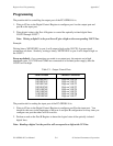
The register bit map shows a diagram of the register with the MSB (bit 7 for an 8-bit register) on
the left and the LSB (bit 0) on the right. Each bit is represented by a square with the bit name
inside. An asterisk (*) after the bit name indicates that the bit is inverted (negative logic). An X
represents a don’t care state; in other words, the logic may be digital 0 or 1.
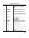
Digital I/O Register Group
Digital I/O on the PC-OPDIO-16 uses an 82C55A integrated circuit. Two of the ports, port A
and port B, are used in the PC-OPDIO-16; port A is for output, and port B is for input.
Bit descriptions for the registers in the Configuration and Calibration Register Group are given
on the following pages.
Note: Interrupts are not supported on the PC-OPDIO-16.
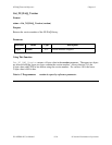
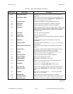
Port A Register
The Port A Register can be written to in order to control the eight optically isolated digital output
lines. Reading the Port A Register returns the logic state of the eight digital lines, PA<0..7>,
constituting port A.
Address: Base address + 00 (hex)
Type: Read-and-write
Word Size: 8-bit
Bit Map:
76543210
D7 D6 D5 D4 D3 D2 D1 D0
Bit Name Description
7–0 D<7..0> Data—These are 8-bit port A data.