


A-6 681XXC OM
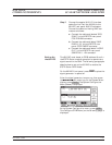
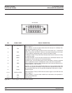
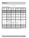
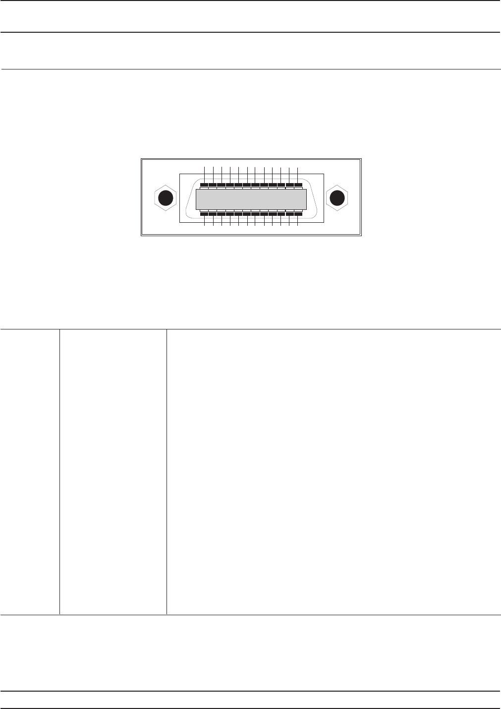
IEEE-488 GPIB
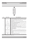
13 14 15 16 17 18 19 20 21 22 23 24
123456789
10 11 12
PIN SIGNAL NAME SIGNAL DESCRIPTION
1-4 DIO 1 thru DIO 4
Data Input/Output: Bits are HIGH when the data is logical 0 and LOW when the
data is logical 1.
5 EOI
End or Identify: A low-true state indicates that the last byte of a multibyte mes-
sage has been placed on the line.
6DAV
Data Valid: A low-true state indicates that the active talker has (1) sensed that
NRFD is high-false and NDAC is low-true, (2) placed the data byte on the bus,
and (3) waited an appropriate length of time for the data to settle.
7 NRFD
Not Ready For Data: Ahigh-false state indicates that all active listeners are ready
to accept new data.
8 NDAC
Not Data Accepted: A low-true state indicates that all addressed listeners have
accepted the current data byte for internal processing.
9 IFC
Interface Clear: A low-true state places all bus instruments in a known, quiescent
state—unaddressed to talk, unaddressed to listen, and service request idle.
10 SRQ
Service Request: A low-true state indicates that a bus instrument desires the im
-
mediate attention of the controller.
11 ATN
Attention: A low-true state indicates that the bus is in the command mode (data
lines are carrying bus commands). A high-false state indicates that the bus is in
the data mode (data lines are carrying device-dependent instructions or data).
12 Shield Chassis Ground
13-16 DIO5 thru DIO6
Data Input/Output: Bits are HIGH when the data is logical 0 and LOW when the
data is logical 1.
17 REN
Remote Enable: A low-true state enables bus instruments to be operated re
-
motely, when addressed.
18-24 GND Logic Ground
Figure A-3. Pinout Diagram, IEEE-488 GPIB Connector
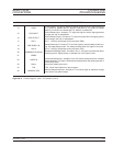
REAR PANEL CONNECTOR
CONNECTORS PINOUT DIAGRAMS