


HD151TS207SS
Rev.1.00, Apr.25.2003, page 7 of 38
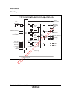
I
2
C Controlled Register Bit Map
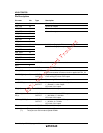
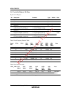
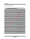
Byte0 Control Register
Bit Description Contents Type Default Note
7 Reserved R 0
6 Reserved R 0
5 Reserved R 0
4 Reserved R 0
3 PCI_Stop Reflects the current value
of the external PCI_STOP# pin
0 = PCI_STOP# pin is Low
1 = PCI_STOP# pin is High
RX
2 Reserved R X
1 FS_B Reflects the value of the
FS_B pin sampled on power up
0 = FS_B Low at power up
1 = FS_B High at power up
RX
0 FS_A Reflects the value of the
FS_A pin sampled on power up
0 = FS_A Low at power up
1 = FS_A High at power up
RX
See
Table
1
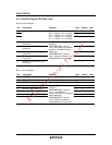
Table1 Clock Frequency Function Table
Byte6
Bit5
FS_A FS_B CPU
[MHz]
SRC
[MHz]
3V66
[MHz]
PCIF
PCI
[MHz]
REF0
REF1
[MHz]
USB
DOT
[MHz]
Note
0 0 0 100 100/200 66 33 14.318 48
0 0 1 200 100/200 66 33 14.318 48
0 1 0 133 100/200 66 33 14.318 48
0 1 1 166 100/200 66 33 14.318 48
1 0 0 200 100/200 66 33 14.318 48
1 0 1 400 100/200 66 33 14.318 48
1 1 0 266 100/200 66 33 14.318 48
1 1 1 333 100/200 66 33 14.318 48
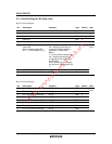
Table2 Test Clock select table
TEST_CLK# CPU
[MHz]
SRC
[MHz]
3V66
[MHz]
PCIF
PCI
[MHz]
REF0
REF1
[MHz]
USB
DOT
[MHz]
Note
1 REF/2 REF/2 REF/4 REF/8 REF REF/2
0 Hi–Z Hi–Z Hi–Z Hi–Z Hi–Z Hi–Z
See Note1,
Table3
Note: 1. REF is a clock over driven on the XIN during test mode.