


HD151TS207SS
Rev.1.00, Apr.25.2003, page 5 of 38
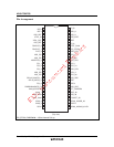
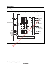
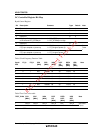
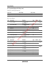
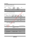
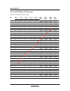
Pin Descriptions (cont.)
Pin name No. Type Description
PWRDWN#/
SAFE_F#
21 INPUT
PULL–UP*
PWRDWN# / SAFE_F# selectable input.
Default is PWRDWN# input.
Byte15[5] = “1” : SAFE_F# input.
PWRDWN# is all clocks stop pin.
Asynchronous active “Low” input.
When asserted low, all output clocks are disabled.
SAFE_F# is active “Low” input.
When SAFE_F# is “Low” ,frequency mode is changed to the
predefined frequency mode.
3V66_0/RESET# 22 OUTPUT 3V66 / Watchdog RESET# selectable output.
Default is 3V66 output.
This signal is active low and selected by Mode latch input.
3V66_[1:3] 23,26,
27
OUTPUT 3V66 clock 3.3V outputs.
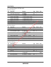
SCLK 28 INPUT
PULL-UP*
Clock input for I
2
C logic.
**SEL66_48/
3V66_4/VCH
29 INPUT/
OUTPUT
Latched select input for 3V66/VCH output 1 = 48 MHz,
0 = 66.66 MHz. /3V66 or VCH clock output.
SDATA 30 IN/OUTPUT
PULL-UP*
Data input for I
2
C logic.
**SEL48_24/
USB_48
31 INPUT/
OUTPUT
Latched select input for 48_24 MHz output
1 = 24 MHz, 0 = 48 MHz / 24_48 MHz clock 3.3 V output.
FS3/DOT_48 32 INPUT/
OUTPUT
Frequency select latch input pin.
/DOT_48 clock 3.3 V output.
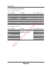
VTT_PWRGD# 35 INPUT
PULL-UP*
Qualifying input that latches FS_A and FS_B.
When asserted low, FS_A and FS_B are latched.
SRC# 37 OUTPUT “Complementary” clock of Differential Serial Reference Clock.
SRC 38 OUTPUT “True” clock of Differential Serial Reference Clock.
CPU_[0:2]# 40,43,
46
OUTPUT “Complementary” clock of differential CPU clock.
CPU_[0:2] 41,44,
47
OUTPUT “True” clock of differential CPU clock.
PCI_STOP# 49 INPUT
PULL–UP*
PCI clocks stop pin. Active “Low” input.
When asserted low, PCI[6:0] and SRC clocks are
synchronously disabled in low state.
Usually this pin does not give to effect PCIF[2:0] clock outputs.
TEST_CLK# 50 INPUT
PULL-UP*
Test clock mode pin. Active “Low” input.
FS_[A:B] 51,52 INPUT CPU clocks frequency select latch input.
IREF 52 INPUT A precision resistor is attached to this pin which is connected
to internal current reference.
A resistor is connected between this pin and GNDIREF.
Note: (*): Those pins are 150 kΩ internal pulled-UP.
(**): Those pins are 150 kΩ internal pulled-DOWN