


HD151TS207SS
Rev.1.00, Apr.25.2003, page 23 of 38
I
2
C Controlled Register Bit Map (cont.)
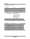
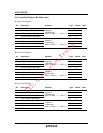
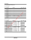
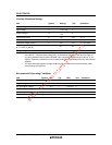
Byte28 Control Register
Bit Description Contents Type Default Note
7 Reserved 0 = Normal, 1 = Late R/W 0
6 PCI_6 Skew Select Bit 0 = Normal, 1 = Late R/W 0
5 PCI_5 Skew Select Bit 0 = Normal, 1 = Late R/W 0
4 PCI_4 Skew Select Bit 0 = Normal, 1 = Late R/W 0
3 PCI_3 Skew Select Bit 0 = Normal, 1 = Late R/W 0
2 PCI_2 Skew Select Bit 0 = Normal, 1 = Late R/W 0
1 PCI_1 Skew Select Bit 0 = Normal, 1 = Late R/W 0
0 PCI_0 Skew Select Bit 0 = Normal, 1 = Late R/W 0
See
Note
1
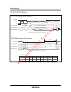
Note: 1. Normal = Skew1(B26[3:0]), Late = Skew1(B26[3:0]) +Skew2 (B26[7:4]).
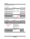
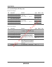
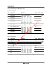
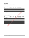
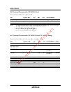
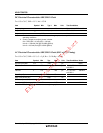
Byte29 Control Register
Bit Description Contents Type Default Note
7 VCH Slew Rate Control Bit1 R/W 1
6 VCH Slew Rate Control Bit0
00 = Normal, 10 = “++”
01 = “+“ , 11 = “–”
R/W 0
5 PCI Slew Rate Control Bit1 R/W 1
4 PCI Slew Rate Control Bit0
00 = Normal, 10 = “++”
01 = “+“ , 11 = “–”
R/W 0
3 PCIF Slew Rate Control Bit1 R/W 1
2 PCIF Slew Rate Control Bit0
00 = Normal, 10 = “++”
01 = “+“ , 11 = “–”
R/W 0
1 3V66 Slew Rate Control Bit1 R/W 1
0 3V66 Slew Rate Control Bit0
00 = Normal, 10 = “++”
01 = “+“ , 11 = “–”
R/W 0