HD151TS207SS
Rev.1.00, Apr.25.2003, page 14 of 38
I
2
C Controlled Register Bit Map (cont.)
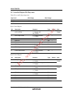
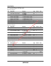
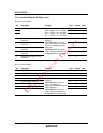
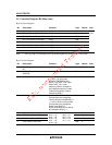
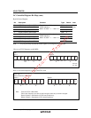
Byte10 Control Register
Bit Description Contents Type Default Note
7 RW 0
6 RW 0
5
SSC Spread Select Bit[2:0] Bit[2:0] =
000 = –0.500%, 100 = ±0.250%
001 = –0.750%, 101 = ±0.375%
010 = –1.000%, 110 = ±0.500%
011 = –1.500%, 111 = ±0.750%
RW 0
4 Backup of latch Input FS_4 at
Power ON
RX
3 Backup of latch Input FS_3 at
Power ON
RX
2 Backup of latch Input FS_2 at
Power ON
RX
1 Backup of latch Input FS_A at
Power ON
RX
0 Backup of latch Input FS_B at
Power ON
When SAFE_F# is Enable
(B15[5]=1)
PWRDWN#/SAFE_F# pin to
“Low”, and if B23[1]=0, frequency
selection is changed to these
setting and
PWRDWN#/SAFE_F# pin to
“High”, frequency selection is
changed back to the last mode.
RX
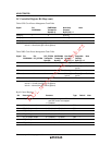
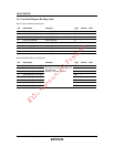
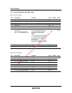
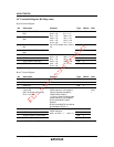
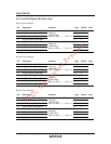
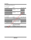
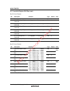
Byte11 Control Register
Bit Description Contents Type Default Note
7 PCI_STOP# Enable Control Bit 0 = Enable , 1 = Disable RW 0
6 CPU_STOP# Enable Control Bit 0 = Enable , 1 = Disable RW 0
5 PWRDWN# Enable Control Bit 0 = Enable , 1 = Disable RW 0
4 Backup of B9[5] written by I
2
CRX
3 Backup of B9[4] written by I
2
CRX
2 Backup of B9[3] written by I
2
CRX
1 Backup of B9[2] written by I
2
CRX
0 Backup of B9[1] written by I
2
C
When SAFE_F# is Enable
(B15[5]=1)
PWRDWN#/SAFE_F# pin to
“Low”, and if B23[1]=1,
frequency selection is changed to
these setting and
PWRDWN#/SAFE_F# pin to
“High”, frequency selection is
changed back to the last mode.
RX


