HD151TS207SS
Rev.1.00, Apr.25.2003, page 21 of 38
I
2
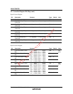
C Controlled Register Bit Map (cont.)
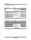
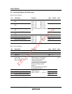
Byte24 Control Register
Bit Description Contents Type Default Note
7 Reserved R/W 0
6 PCI_STOP# Stop PCI_6
Control Bit
0 = Stoppable, 1 = Free running R/W 0
5 PCI_STOP# Stop PCI_5
Control Bit
0 = Stoppable, 1 = Free running R/W 0
4 PCI_STOP# Stop PCI_4
Control Bit
0 = Stoppable, 1 = Free running R/W 0
3 PCI_STOP# Stop PCI_3
Control Bit
0 = Stoppable, 1 = Free running R/W 0
2 PCI_STOP# Stop PCI_2
Control Bit
0 = Stoppable, 1 = Free running R/W 0
1 PCI_STOP# Stop PCI_1
Control Bit
0 = Stoppable, 1 = Free running R/W 0
0 PCI_STOP# Stop PCI_0
Control Bit
0 = Stoppable, 1 = Free running R/W 0
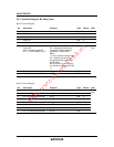
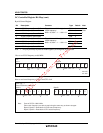
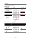
Byte25 Control Register
Bit Description Contents Type Default Note
7 CPU Clock Skew1 Control
Bit3
R/W 1
6 CPU Clock Skew1 Control
Bit2
R/W 0
5 CPU Clock Skew1 Control
Bit1
R/W 0
4 CPU Clock Skew1 Control
Bit0
Delay Ahead
1000 = +0.00ns, 0111 = –0.20ns
1001 = +0.20ns, 0110 = –0.40ns
1010 = +0.40ns, 0101 = –0.60ns
1011 = +0.60ns, 0100 = –0.80ns
1100 = +0.80ns, 0011 = –1.00ns
1101 = +1.00ns, 0010 = –1.20ns
1110 = +1.20ns, 0001 = –1.40ns
1111 = +1.40ns, 0000 = –1.60ns
R/W 0
See
Note
1
3 CPU Clock Skew2 Control
Bit3
R/W 1
2 CPU Clock Skew2 Control
Bit2
R/W 0
1 CPU Clock Skew2 Control
Bit1
R/W 0
0 CPU Clock Skew2 Control
Bit0
Delay Ahead
1000 = +0.00ns, 0111 = –0.15ns
1001 = +0.15ns, 0110 = –0.30ns
1010 = +0.30ns, 0101 = –0.45ns
1011 = +0.45ns, 0100 = –0.60ns
1100 = +0.60ns, 0011 = –0.75ns
1101 = +0.75ns, 0010 = –0.90ns
1110 = +0.90ns, 0001 = –1.05ns
1111 = +1.05ns, 0000 = –1.20ns
R/W 0
See
Note
1
Note: 1. Total CPU Clock Skew is Skew1+Skew2.


