


HD151TS207SS
Rev.1.00, Apr.25.2003, page 16 of 38
I
2
C Controlled Register Bit Map (cont.)
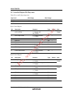
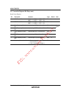
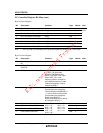
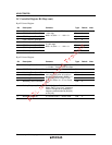
Byte14 Control Register
Bit Description Contents Type Default Note
7 Reserved R/W 0
6 PLL1 M1 Divider Control Bit6 M1[6] R/W 0
5 PLL1 M1 Divider Control Bit5 M1[5] R/W 0
4 PLL1 M1 Divider Control Bit4 M1[4] R/W 1
3 PLL1 M1 Divider Control Bit3 M1[3] R/W 0
2 PLL1 M1 Divider Control Bit2 M1[2] R/W 0
1 PLL1 M1 Divider Control Bit1 M1[1] R/W 1
0 PLL1 M1 Divider Control Bit0 M1[0] R/W 0
See
Note
1
Note: 1. B12[1:0], B13[7:0] and B14[6:0] must be written together (at writing B14) in every case.
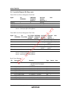
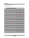
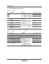
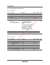
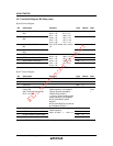
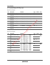
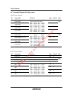
Byte15 Control Register
Bit Description Contents Type Default Note
7 PCI_5 Output Frequency Select
Bit
0 = 33.3 MHz, 1 = 25 MHz R/W 0
6 USB_48 Output Frequency
Select Bit
0 = 48MHz, 1 = 24 MHz R/W 0
5 SAFE_F# Input mode select Bit 0 = PWRDWN# input mode
1 = SAFE_F# input mode
Default is PWRDWN# input.
SAFE_F# is active “Low” input.
When SAFE_F# is “Low”,
frequency mode is changed to
the predefined frequency mode.
Predefined frequency mode is
selected by B23[1].
R/W 0
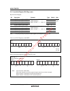
4 Clock Divider Control Bit 0 = Normal mode
Clock dividers are changed by
Table 5 selection decided B9[5:1]
1 = Over or Down clocking mode
Clock dividers are changed by
B15[3:0] and B16[7:0].
B15[3:0] and B16[7:0] are able to
be changed at B15[4] = 1.
R/W 0
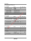
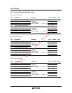
3 CPU Divider Control Bit3 R/W X
2 CPU Divider Control Bit2 R/W X
1 CPU Divider Control Bit1 R/W X
0 CPU Divider Control Bit0
0001 = 1/1,
0010 = 1/2,
0011 = 1/3,
0100 = 1/4,
0101 = 1/5,
0110 = 1/6,
0111 = 1/7
1000 = 1/8
1001 = 1/9
1010 = 1/10
1011 = 1/11
R/W X