


Service Addendum 25
Chapter 4 Differences
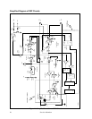
Digital Signal Processor (DSP) Board
The DSP board replaces the Secondary Interface section of the A1 Main PC board. It replaces the
Secondary Microprocessor (U504), the CV and CC programming DACs, Readback D/A, DAC Reference,
Readback Comparators, and the Fan and Overvoltage PWMs. It replaces everything found in Figure 6-5,
sheet 3 plus the OV filter/buffer (U603) found on sheet 2.
The DSP board contains the new Secondary Microprocessor circuits, the CV, CC, OV, OC and Fan DAC’s,
The readback circuits and the secondary ROM and RAM. When operating in the Fixed mode, the instrument
acts like a normal power supply with typical crossover characteristics between CV and CC operation. When
in SAS mode the customer specified I/E operating curve is entered into the secondary RAM where it is used
to modify the supply’s crossover characteristics.
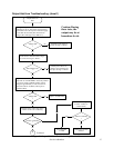
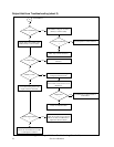
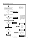
Troubleshooting is to be performed in the Fixed (turn-on default) mode only. See Figure 6-10 for the
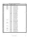
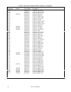
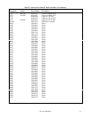
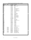
A5J721/A5J722 connector DAC and Bias voltage pin-outs.
Note The DSP board is available as a replacement assembly only. It is not intended to be repaired to the
component level.
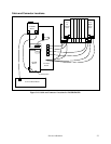
The following figure is a simplified diagram that shows the circuits located on the DSP board (also referred
to as the Secondary Interface) in relation to the Output Power and Control circuits previously discussed in
chapter 4.