


31
Transit case Part number 9211-1296
10 MHz input Accepts a 1, 2, 5, or 10 MHz ±10 ppm [standard timebase]
or ±1 ppm [high-stability timebase] reference signal for
operation with an external timebase. Nominal input
level –3.5 to +20 dBm, impedance 50 ohms.
[BNC, rear panel]
10 MHz output Outputs the 10 MHz reference signal. Level nominally
+3.9 dBm ±2 dB. Nominal output impedance 50 ohms.
[BNC, rear panel]
Alternate power input Accepts CMOS
1
signal for synchronization of external
data and alternate power signal timing. The damage
levels are –0.5 to +5.5 V. [Auxiliary I/O connector,
rear panel]
Baseband generator Accepts 0 to +20 dBm sinewave, or TTL squarewave,
reference input to use as reference clock for the baseband generator.
Phase locks the internal data generator to the external
reference; the RF frequency is still locked to the 10 MHz
reference. Rate is 250 kHz to 100 MHz, 50 ohms
nominal, AC coupled. [BNC, rear panel]
Burst gate input The burst gate in connector accepts a CMOS
1
signal for gating burst power in digital modulation
applications. The burst gating is used when you are
externally supplying data and clock information. The
input signal must be synchronized with the external data
input that will be output during the burst. The burst
power envelope and modulated data are internally
delayed and re-synchronized. The input signal must be
CMOS high for normal burst RF power or CW RF output
power and CMOS low for RF off. The damage levels
are –0.5 to +5.5 V.
This female BNC connector is provided on signal
generators with Option 601 or 602. On signal generators
with Option 1EM, this input is relocated to a rear panel
SMB connector. With Option 401, this connector is used
for the even second synchronization input.
Coherent carrier output
2
Outputs RF modulated with FM or FM, but not IQ,
pulse or AM. Nominal power –2 dBm ±5 dB. Nominal
impedance 50 ohms. Frequency range from > 250 MHz
to 4 GHz. For RF carriers below this range, output
frequency = 1 GHz – frequency of RF output. Damage
levels 20 VDC and 13 dBm reverse RF power.
[SMA, rear panel]
Accessories
1. Rear panel inputs and outputs are 3.3 V CMOS, unless indicated otherwise. CMOS inputs will accept 5 V CMOS, 3 V CMOS, or TTL voltage levels.
2. Coherent carrier is modulated by FM or FM when enabled.
General Characteristics
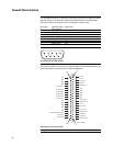
Inputs and outputs
All front panel connectors can be moved
to rear with Option 1EM.