


8 www.xilinx.com Virtex-4 LX/SX Prototype Platform
UG078 (v1.2) May 24, 2006
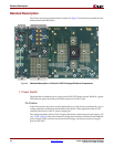
Introduction
R
Features
• Independent power supply jacks for VCCINT, VCCO, and VCCAUX
• Selectable VCCO-enable pins for each SelectIO™ bank
• Configuration port for use with Parallel Cable III and Parallel Cable IV cables
• 32 clock inputs
♦ 4 differential clock pairs
♦ 4 LVTTL-type oscillator sockets
♦ 20 breakout clock pins
• Power indicator LEDs
• Onboard Platform Flash ISPROM (32 Mb) for configuration
• Onboard power supplies for the Platform Flash ISPROM
• JTAG port for reprogramming the XCF32P series reconfigurable ISPROM and the user
FPGA, also known as the device under test (DUT)
• Upstream and downstream System ACE™ connectors and configuration interface
connectors
• Onboard battery holder
• One low-voltage, 14-pin, DIP crystal oscillators
The kit contains headers that can be soldered to the breakout area, if desired. These headers
are useful with certain types of oscilloscope probes for either connecting function
generators or wiring pins to the prototype area.
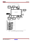
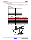
The Virtex-4 prototype platform (the board) contains a DUT FPGA and one In-System
Programmable Configuration PROM (ISPROM). The ISPROM can hold up to 33,554,432
bits. The DUT can be configured either from the ISPROM or from the configuration ports
(Parallel Cable III/IV cable).
In addition to the ISPROM and the configuration ports, there are upstream connectors and
downstream connectors. The upstream connectors can be connected to configure the DUT
by using the System ACE configuration solution or by chaining another board. The
downstream connectors can be used to connect to another board in a chain for serial
configuration. A maximum of two boards can be chained together.