


Virtex-4 LX/SX Prototype Platform www.xilinx.com 11
UG078 (v1.2) May 24, 2006
Detailed Description
R
Off Position
In the OFF position, the power switch disables all modes of powering the DUT.
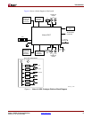
Power Enable Jumpers
For each power supply there are headers marked SUPPLY on one side and JACK on the
other side. Appropriate placements of jumpers on these headers enables delivery of all
power from either the onboard regulators or the three power supply jacks marked
VCCINT, VCCO, and VCCAUX.
2. Power Supply Jacks
One method of delivering power to the DUT is by way of the power supply jacks. (Consult
the Xilinx data book, http://www.xilinx.com/partinfo/datasheet.htm
, for the maximum
voltage rating for each device you are using.) The power supply jacks are:
• VCCINT
♦ Supplies voltage to the V
CCINT
of the DUT
• VCCO
♦ Supplies I/O voltages to the DUT
♦ Each bank can be powered from one of two sources (V
CCO
, V
CCINT
) by
appropriate placement of jumpers on the header
• VCCAUX
♦ Supplies voltage to the V
CCAUX
DUT pins
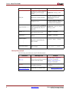
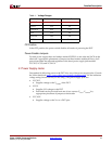
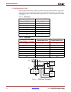
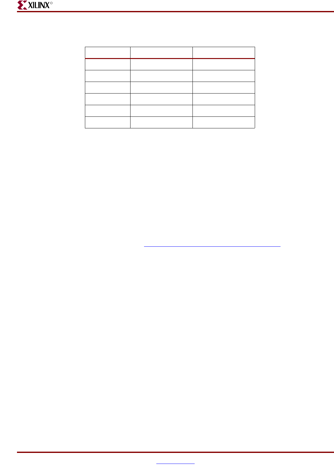
Table 1: Voltage Ranges
Label Maximum Voltage Maximum Current
VCCINT 1.2V 1A
VCCO 3.3V 2A
VCCAUX 2.5V 1.5A
VCC 3.3V 2A
VCC1V8 1.8V 1A
AVCC 2.5V 25 mA