


18 www.xilinx.com Virtex-4 LX/SX Prototype Platform
UG078 (v1.2) May 24, 2006
Detailed Description
R
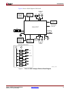
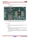
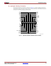
11. Differential Clock Inputs
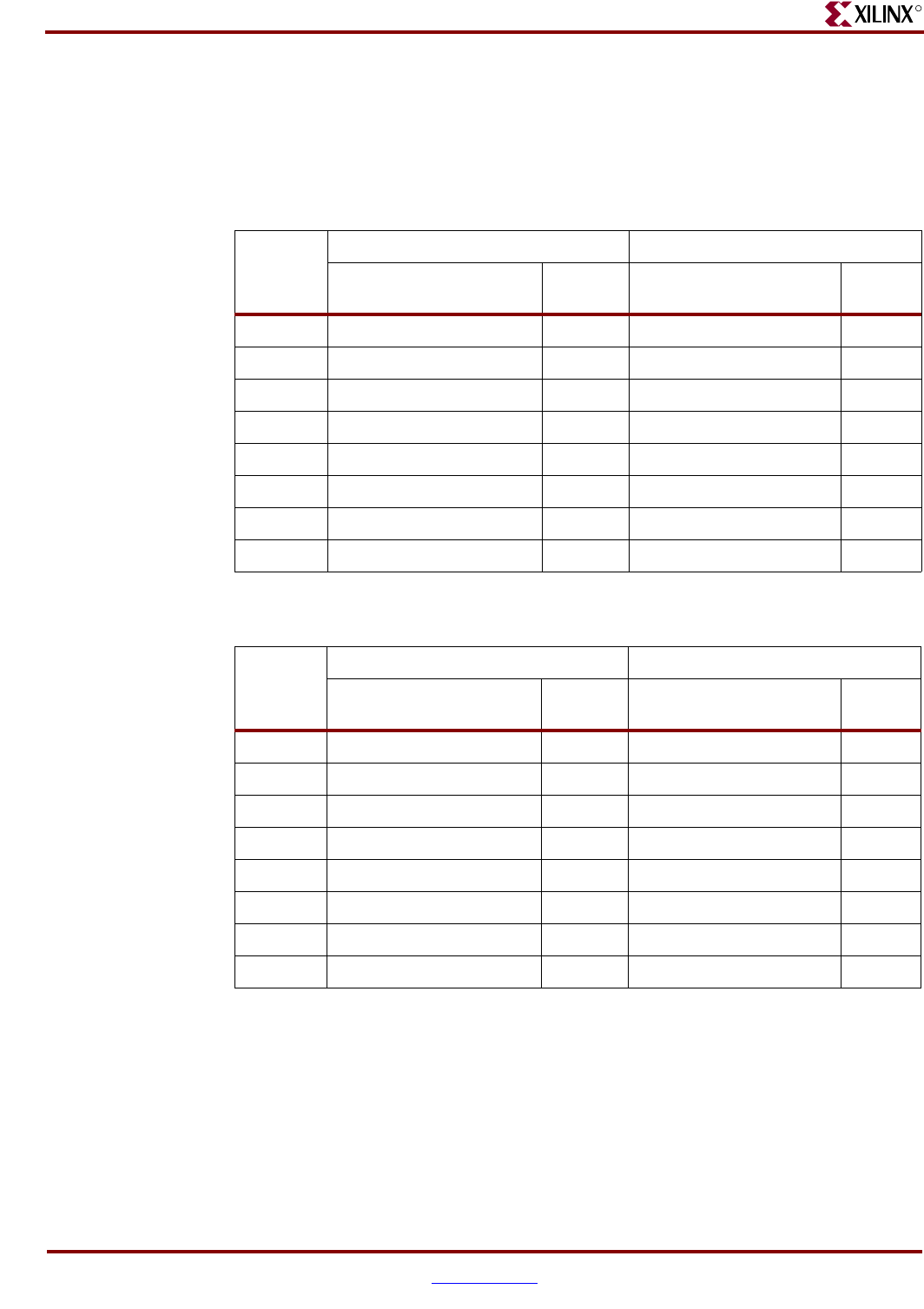
In addition to the oscillator sockets, there are eight 50Ω SMA connectors that allow
connection to an external function generator. These connect to the DUT clock pads as
shown in Table 6 and Table 7. They can also be used as differential clock inputs. The
differential clock pairings (DIFFERENTIAL PAIRS) are as shown in the tables.
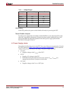
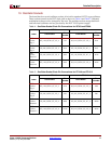
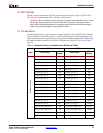
Table 6: SMA Clock Pin Connections for SF363 and FF668
SF363 FF668
Label Clock Name
Pin
Number
Clock Name
Pin
Number
N IO_L8N_GC_LC_3 B7 IO_L8N_GC_LC_3 C12
P IO_L8P_GC_LC_3 A7 IO_L8P_GC_LC_3 C13
N IO_L2N_GC_VRP_LC_3 B9 IO_L2N_GC_VRP_LC_3 A11
P IO_L2P_GC_VRN_LC_3 A10 IO_L2P_GC_VRN_LC_3 A12
N IO_L2N_GC_LC_4 W5 IO_L2N_GC_LC_4 AB10
P IO_L2P_GC_LC_4 Y5 IO_L2P_GC_LC_4 AC10
N IO_L8N_GC_CC_LC_4 W8 IO_L8N_GC_CC_LC_4 AD11
P IO_L8P_GC_CC_LC_4 W9 IO_L8P_GC_CC_LC_4 AD12
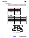
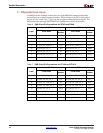
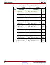
Table 7: SMA Clock Pin Connections for FF1148 and FF1513
FF1148 FF1513
Label Clock Name
Pin
Number
Clock Name
Pin
Number
N IO_L8N_GC_CC_LC_3 G16 IO_L8N_GC_CC_LC_3 K21
P IO_L8P_GC_CC_LC_3 G17 IO_L8P_GC_CC_LC_3 L21
N IO_L2N_GC_VRP_LC_3 J17 IO_L2N_GC_VRP_LC_3 K19
P IO_L2P_GC_VRP_LC_3 H17 IO_L2P_GC_VRP_LC_3 J19
N IO_L2N_GC_LC_4 AF16 IO_L2N_GC_LC_4 AF18
P IO_L2P_GC_LC_4 AG16 IO_L2P_GC_LC_4 AF19
N IO_L8N_GC_CC_LC_4 AH17 IO_L8N_GC_CC_LC_4 AJ19
P IO_L8P_GC_CC_LC_4 AJ17 IO_L8P_GC_CC_LC_4 AK19