


Virtex-4 LX/SX Prototype Platform www.xilinx.com 19
UG078 (v1.2) May 24, 2006
Detailed Description
R
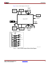
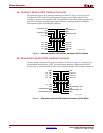
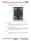
12. DUT Socket
The DUT socket contains the user FPGA, referred to as the device under test (DUT). The
DUT must be oriented using the P1 indicator on the board.
Caution!
Failure to insert the device to the proper orientation can damage the device. To avoid
pin damage, always use the vacuum tool provided when inserting or removing the Virtex-4
device. When using BGA packages, do not apply pressure to the device while activating the
socket. Doing so can damage the socket and/or the device.
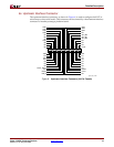
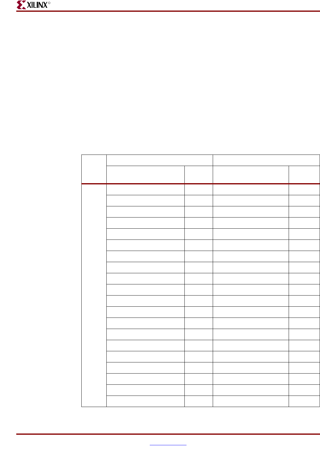
13. Pin Breakout
The pin breakout area is used to monitor or apply signals to each of the DUT pins. Headers
can be soldered to the breakout area to use with certain types of oscilloscope probes, for
either connecting function generators or wiring pins to the pin breakout area. Clocks in the
pin breakout area that connect to the DUT clock pads are shown in Table 8 and Table 9,
page 20.
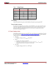
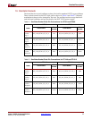
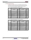
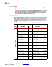
Table 8: Breakout Clock Pin Connections for SF363 and FF668
SF363 FF668
Label Clock Name
Pin
Number
Clock Name
Pin
Number
Breakout Area
IO_L4P_GC_LC_3 B10 IO_L4P_GC_LC_3 B13
IO_L4N_GC_VREF_LC_3 C10 IO_L4N_GC_VREF_LC_3 B12
IO_L5P_GC_LC_3 B13 IO_L5P_GC_LC_3 A16
IO_L5N_GC_LC_3 A13 IO_L5N_GC_LC_3 A15
IO_L6P_GC_LC_3 A8 IO_L6P_GC_LC_3 A10
IO_L6N_GC_LC_3 B8 IO_L6N_GC_LC_3 B10
IO_L7P_GC_LC_3 B14 IO_L7P_GC_LC_3 B17
IO_L7N_GC_LC_3 A14 IO_L7N_GC_LC_3 A17
IO_L3P_GC_LC_3 C11 IO_L3P_GC_LC_3 C14
IO_L3N_GC_LC_3 B11 IO_L3N_GC_LC_3 C15
IO_L4P_GC_LC_4 Y6 IO_L4P_GC_LC_4 AF11
IO_L4N_GC_VREF_LC_4 W6 IO_L4N_GC_VREF_LC_4 AF10
IO_L5P_GC_LC_4 W11 IO_L5P_GC_LC_4 AE14
IO_L5N_GC_LC_4 W10 IO_L5N_GC_LC_4 AE13
IO_L6P_GC_LC_4 Y7 IO_L6P_GC_LC_4 AE10
IO_L6N_GC_LC_4 W7 IO_L6N_GC_LC_4 AD10
IO_L7P_GC_VRN_LC_4 Y10 IO_L7P_GC_VRN_LC_4 AD17
IO_L7N_GC_VRP_LC_4 Y9 IO_L7N_GC_VRP_LC_4 AD16
IO_L3P_GC_CC_LC_4 Y12 IO_L3P_GC_CC_LC_4 AB17
IO_L3N_GC_CC_LC_4 Y11 IO_L3N_GC_CC_LC_4 AC17