


Frequency Generator for the Spartan-3E Starter Kit 7
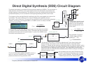
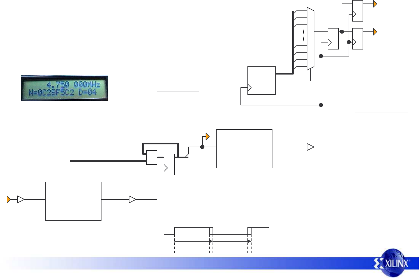
Direct Digital Synthesis (DDS) Circuit Diagram
32-Bit
Counter
CLKIN
50MHz
clk
BUFG
phase_acc_dcm
DCM
The first DCM is used to multiply the 50MHz clock by a
factor or 4 and form a 200MHz clock. This gives the
phase accumulator a timing resolution of 5ns.
CLKFX
CLKFX_MULTIPLY=4
CLKFX_DIVIDE=1
clk_200mhz dds_clk
BUFG
200MHz
+
dds_control_word[31:0]
phase_accumulator[31:0]
phase_acc
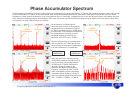
The phase accumulator is a standard 32-bit accumulator operating at 200MHz. This accumulator is
really the heart of the DDS as it is the most significant bit of the accumulator that produces the
variable frequency being synthesized. The remaining circuits only multiply, divide and clean this
synthesized frequency or are involved with selecting and generating the DDS control words.
The frequency of the most significant bit is defined by the 32-bit value applied to the input of the
accumulator. This value is shown as ‘N’ on the LCD display and is applied to the bus
‘dds_control_word’ in the circuit. The value of N is computed in such a way that the synthesized
frequency is nominally in the range 6.25MHz to 12.5MHz so that it is always a suitable
input to the second DCM.
[31]
N × 200MHz
F
MSB
=
2
32
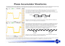
In this example N=204010946 decimal so the output from the phase accumulator
is ~9.5MHz (a period of approximately 105ns). That means that the accumulator
synthesizes one output cycle for approximately 21 cycles of the 200MHz clock
from which the accumulator runs.
CLKIN
BUFG
frequency_aligned_dcm
DCM
CLKFX
CLKFX_MULTIPLY=256
CLKFX_DIVIDE=16
dcm_clean_clk
synth_clk
The second DCM is used in a ‘frequency aligned mode’. At the time of writing this
reference design, this mode is not an officially documented or supported feature.
However, it is hoped that this reference design will enable you to see this mode in action
and evaluate it for yourself. In this mode, the DCM not only multiplies the input clock, but
also has the effect of reducing cycle to cycle jitter. This is because the normal phase
alignment mode of the DCM has been disabled and the DCM is tracking the average of
the input frequency instead.
×4
×16
10 or 11
cycles
10 or 11
cycles
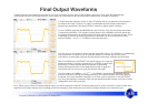
In the example, the input to the DCM will have 5ns
of cycle to cycle jitter as the square wave is formed
from 21 cycles of 200MHz. The DCM will generate
~153MHz square wave with <300ps of jitter.
frequency_divider[31:0]
freq_scaling
0
1
2
3
30
31
29
N
D
io9
io12
sma_out
dds_scaling_word
A simple binary counter is used
to divide the low jitter clock by
powers of 2 and a multiplexer
selects the appropriate course
division factor.
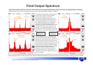
N × 200MHz × 16
F
O
=
2
(D+1)
× 2
32
In the example, D=4 so the
~153MHz from the DCM is
divided by 2
(4+1)
=32
F
O
=4.7499999869MHz