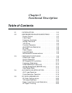
Chapter 2
Functional Description
2-1 INTRODUCTION This chapter provides brief functional descriptions of the major sub
-
systems that are contained in each model of the Series 682XXB/
683XXB Synthesized Signal Generators. In addition, the operation of
the frequency synthesis, automatic level control (ALC), and RF deck
subsystems is described so that the reader may better understand the
overall operation of the instrument. Block diagrams are included to
supplement the written descriptions.
2-2 682XXB/683XXB MAJOR
SUBSYSTEMS
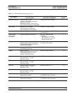
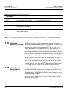
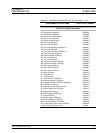
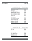
The 682XXB/683XXB circuitry consists of various distinct subsystems
that are contained on one or more printed circuit board (PCB) assem-
blies or in microwave components located on the RF deck. The follow-
ing paragraphs identify the subsystems that make up the instrument
and provide a brief description of each. Figure 2-1 (page 2-6) is an
overall block diagram of a typical 682XXB/683XXB.
NOTE
Identical model numbers of the series 682XXB signal gen-
erator and series 683XXB signal generator contain the same
major subsystems. The only functional difference between
the two series is that the series 683XXB signal generator
has the additional capability of generating analog frequency
sweeps. This functional difference between the series is
noted in the following descriptions where applicable.
Digital
Control
This circuit subsystem consists of the A17 CPU and
A16 CPU Interface PCBs. The central processor unit
(CPU) is the main controller for the 682XXB/
683XXB. This controller directly or indirectly con
-
trols all functions of the instrument. The CPU con
-
tains memory that stores the main operating system
components and instrument firmware, instrument
calibration data, and front panel setups in the
power-off condition. It has a GPIB interface that al
-
lows it to communicate with external devices over
the GPIB and it has a serial interface to a serial ter
-
minal port on the rear panel. The CPU is directly
linked via a dedicated data and address bus to the
A2 Front Panel PCB, the A8 Function Generator
PCB, the A9 PIN Control PCB, the A10 ALC PCB,
the A11 FM PCB, the A12 Analog Instruction PCB,
and the A16 CPU Interface PCB.
682XXB/683XXB MM 2-3


