


GE863-PRO
3
Hardware User Guide
1vv0300773a Rev. 0 - 24/01/08
Reproduction forbidden without Telit Communications S.p.A. written authorization - All Rights Reserved page 34 of 64
This line of transmission shall fulfil the following requirements:
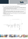
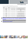
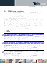
ANTENNA LINE ON PCB REQUIREMENTS
Impedance
50 ohm
Max Attenuation
0,3 dB
No coupling with other signals allowed
Cold End (Ground Plane) of antenna shall be equipotential to
the GE863-PRO
3
ground pins
Furthermore if the device is developed for the US market and/or Canada market, it shall comply to the
FCC and/or IC approval requirements:
This device is to be used only for mobile and fixed application. The antenna(s) used for this transmitter
must be installed to provide a separation distance of at least 20 cm from all persons and must not be
co-located or operating in conjunction with any other antenna or transmitter. End-Users must be
provided with transmitter operation conditions for satisfying RF exposure compliance. OEM integrators
must ensure that the end user has no manual instructions to remove or install the GE863-PRO
3
module. Antennas used for this OEM module must not exceed 3dBi gain for mobile and fixed
operating configurations.
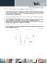
6.2 GSM Antenna - PCB line Guidelines
• Ensure that the antenna line impedance is 50 ohm;
• Keep the antenna line on the PCB as short as possible, since the antenna line loss shall be less
than 0,3 dB;
• Antenna line must have uniform characteristics, constant cross section, avoid meanders and
abrupt curves;
• Keep, if possible, one layer of the PCB used only for the Ground plane;
• Surround (on the sides, over and under) the antenna line on PCB with Ground, avoid having other
signal tracks facing directly the antenna line track;
• The ground around the antenna line on PCB has to be strictly connected to the Ground Plane by
placing vias once per 2mm at least;
• Place EM noisy devices as far as possible from GE863-PRO
3
antenna line;
• Keep the antenna line far away from the GE863-PRO
3
power supply lines;
• If you have EM noisy devices around the PCB hosting the GE863-PRO
3
, such as fast switching
ICs, take care of the shielding of the antenna line by burying it inside the layers of PCB and
surround it with Ground planes, or shield it with a metal frame cover.
• If you don't have EM noisy devices around the PCB of GE863-PRO
3
, by using a strip-line on the
superficial copper layer for the antenna line, the line attenuation will be lower than a buried one;