© National Instruments Corporation 23 NI 5421 Specifications
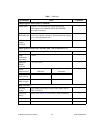
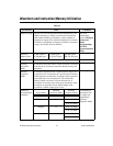
Output Signal Characteristics (Continued)
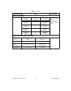
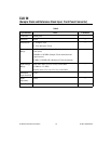
Output Skew Typical: 1 ns, maximum 2 ns. Skew between any
two outputs on the DIGITAL DATA & CONTROL
front panel connector.
—
Output
Enable/Disable
Controlled through the software on all Data Output Signals
and Control Signals collectively. When disabled, the outputs
go to a high-impedance state.
—
Maximum
Output
Overload
–0.3 V to +3.9 V —
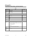
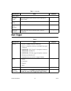
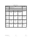
Input Signal Characteristics (Includes DDC CLK IN and PFI<2..3>)
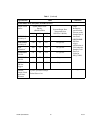
Signal Type LVDS (Low-Voltage Differential Signal) —
Input
Differential
Impedance
100 Ω —
Maximum
Output
Overload
–0.3 V to +3.9 V —
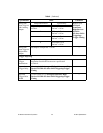
Signal
Characteristics
Minimum Maximum
—
Differential
Input Voltage
0.1 V 0.5 V
Input Common
Mode Voltage
0.2 V 2.2 V
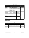
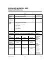
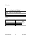
DDC CLK OUT
Clocking
Format
Data outputs and markers change on the falling edge of
DDC CLK OUT.
—
Frequency
Range
Refer to the Sample Clock section for more information. —
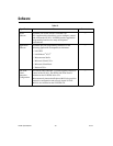
Duty Cycle 40% to 60% —
Jitter 40 ps rms —
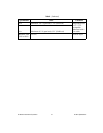
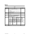
Table 7. (Continued)
Specification Value Comments


